|
|
| RESEARCH ACTIVITIES |
 |
| Luminescence Properties of Group IV (Si, Ge) Semiconductor Nanocrystals |
 |
168. Kei Ueda, Takeshi Tayagaki, Masatoshi Fukuda, Minoru Fujii, and Yoshihiko Kanemitsu,
Breakdown of the k-conservation rule in quantized Auger recombination in Si1-xGex nanocrystals
Physical Revew B 86, 155316, pp. 1-5 (2012). |
| Dynamics of quantized Auger recombination in Si1−xGex nanocrystals (NCs)
embedded in SiO2 films was studied by femtosecond intraband pump-probe
spectroscopy. The temporal change of the electron-hole pair number under
strong photoexcitation was well explained by the quantized Auger recombination
model that considered the size distribution of NCs. On the basis of the
dependence of the Auger decay rate on temperature and Ge composition, we
confirmed the occurrence of breakdown of the k-conservation rule in quantized
Auger recombinationinSiandSi1−xGex NCs. |
|
|
|
| |
155. Ilya Sychugov, Jan Valenta, K. Mitsuishi, Minoru Fujii, and Jan Linnros,
Photoluminescence measurements of zero-phonon optical transitions in silicon nanocrystals
Physical Review B, Vol. 84, 125326, pp. 1-5 (2011).
|
| Optical transitions in silicon nanocrystals with different surface passivations
were probed at low temperatures on a single-particle level. A type of quasidirect
recombination process, different from the quantum-confined exciton transition,
is identified. The luminescence spectra have different emission energies,
but the contribution of a no-phonon transition is significantly higher
than expected from the quantum-confinement model. Its relative strength
was found to be temperature dependent, suggesting spatial localization
of excitons as a possible origin. |
|
 |
123. Yugo Mochizuki, Minoru Fujii, Shinji Hayashi, Takaaki Tsuruoka, and Kensuke Akamatsu
“Enhancement of Photoluminescence from Silicon Nanocrystals by Metal Nanostructures made by Nanosphere Lithography,”
Journal of Applied Physics, Vol. 106, 013517, pp. 1-5 (2009). |
| The effect of metal nanostructures prepared by nanosphere lithography on photoluminescence (PL) properties of silicon nanocrystals (Si-ncs) is studied. By placing Ag nanotriangles or Au nanovoids on SiO2 films containing Si-ncs, the PL intensity is enhanced. For the sample having Ag nanotriangles, the largest PL enhancement is obtained when the excitation wavelength coincides with the absorption band of Ag nanotriangles. This suggests that the enhancement of the incident field by surface plasmon polariton (SPP) excitation is responsible for the PL enhancement. On the other hand, for the sample having Au nanovoids, the PL enhancement is mainly made by the enhancement of effective radiative decay rate of Si-ncs by efficient excitation and scattering of SPPs. |
|
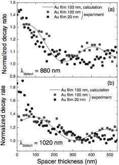 |
95. Toshihiro Nakamura, Minoru Fujii, Satoru Miura, Masaki Inui, and Shinji Hayashi,
"Spontaneous Emission Rate of Si Nanocrystals on Thin Au Film,”
Japanese Journal of Applied Physics, Vol. 46, No. 10A, pp. 6498-6502, October (2007). |
| The effect of Au films with different thicknesses (20 and 100 nm) on the
luminescence decay rate of Si nanocrystals was studied in a wide wavelength
range. For the sample with the Au thickness of 100 nm, the luminescence
decay rate oscillated depending on the distance between the Si nanocrystals
and the Au film owing to the modification of the photonic mode density
at the position of the Si nanocrystals. On the other hand, when the thickness
of the Au film was 20 nm, the oscillation was not observed and a strong
enhancement of the decay rate appeared in a small distance range. The degree
of enhancement depended on the emission wavelength. These effects are considered
to arise from a strong coupling between the electronic excitation of Si
nanocrystals and the surface plasmon polariton modes supported by the rough
Au surface. |
|
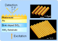 |
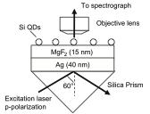
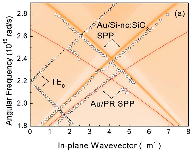
93. Eiji Takeda, Minoru Fujii, Toshihiro Nakamura, Yugo Mochizuki, and Shinji Hayashi,
"Enhancement of Photoluminescence from Excitons in Silicon Nanocrystals via Coupling to Surface Plasmon Polaritons,”
Journal of Applied Physics, Vol. 102, pp. 023506-1-6, July (2007). |
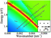
| The enhancement of photoluminescence (PL) is demonstrated from silicon
nanocrystals (Si-ncs) by strong coupling of excitons to surface plasmon
polaritons (SPPs) supported by a Au thin film. SPPs excited via excitons
in Si-ncs were Bragg scattered to photons by one- or two-dimensional gratings,
and strong and directional PL was obtained. From the angular dependence
of PL spectra, dispersion relations of electromagnetic modes involved in
the light emission process were obtained. The overall agreement between
experimentally obtained and theoretically calculated dispersion relations
confirmed that the strong and directional PL is mediated by SPPs. The PL
decay rate of Si-ncs increased by placing a Au thin film on top and the
wavelength dependence of the rate enhancement agreed well with that of
the calculated SPP excitation rate. This suggests that the observed PL
enhancement is due to efficient energy transfer from excitons to SPPs followed
by efficient scattering of SPPs to photons, resulting in the enhancement
of luminescence quantum efficiency. |
|
| |
91. Kimihisa Matsumoto, Minoru Fujii, and Shinji Hayashi,
"Photoluminescence from Si Nanocrystals Embedded in In2O3/SiO2 Glass Thin Films,”
Japanese Journal of Applied Physics, Vol. 46, No. 4A, pp. 1779-1782, April (2007). |
| The photoluminescence (PL) properties of Si nanocrystals embedded in In2O3/SiO2
thin films are studied. The PL properties strongly depend on In and excess
Si concentrations. For the samples with an excess Si concentration larger
than 3.4 at. %, the PL intensity increases as In concentration increases
up to 0.46 at. %, while the PL decay rate is nearly constant. This suggests
that the number of Si nanocrystals contributing to the PL increases. On
the other hand, when the excess Si concentration is low (1.4 at. %), the
PL intensity monotonically decreases with increasing In concentration.
The decrease in the PL intensity is accompanied by the increase in a decay
rate, indicating that the nonradiative recombination process is introduced
by In doping. |
|
 |
86. Eiji Takeda, Toshihiro Nakamura, Minoru Fujii, Satoru Miura, and Shinji Hayashi,
"Surface Plasmon Polariton Mediated Photoluminescence from Excitons
in Silicon Nanocrystals,”
Applied Physics Letters, Vol. 89, 101907, pp. 1-3, September (2006). |
| Surface plasmon polaritons (SPPs) of a metal film can efficiently be excited
when a light emitter is placed nearby. The excited SPPs are converted to
photons by compensating for the momentum mismatch. The authors study SPP-mediated
emission from excitons in Si nanocrystals (Si-nc’s) by placing an organic
grating on a thin Au film placed near Si-nc’s. The dispersion relation
is obtained from angle-resolved photoluminescence measurements, and all
the observed modes are well explained by model calculation. The results
indicate that excitons in Si-nc’s can efficiently excite SPPs in thin metal
films and directed photoluminescence can be realized. |
|
| |
83. Satoru Miura, Toshihiro Nakamura, Minoru Fujii, Masaki Inui, and Shinji Hayashi,
"Size Dependence of Photoluminescence Quantum Efficiency of Si Nanocrystals,”
Physical Review B, vol. 73, pp. 245333-1-5, June (2006). |
| The radiative recombination rate of excitons confined in Si nanocrystals
was modified by placing a Au layer nearby. Oscillation of the rate was
observed when the distance between the active layer and the Au layer was
changed. By comparing the experimentally obtained oscillation behavior
with a calculated one, the radiative and nonradiative recombination rates,
and also the internal quantum efficiency of excitons in Si nanocrystals
were estimated. The relation between the radiative rate and the luminescence
wavelength was on a single curve for all the samples studied. On the other
hand, the nonradiative rate depended strongly on samples. For the samples
annealed at 1250 °C, the estimated quantum efficiency was close to 100%
at longer wavelength side of the luminescence bands, while the maximum
quantum efficiency was 70% for the sample annealed at 1200 °C. The present
results provide evidence that in Si nanocrystal assemblies, the majority
of nanocrystals in samples do not contribute to photoluminescence and a
small part of nanocrystals luminesce with high quantum efficiencies, and
thus the total quantum efficiency is mainly determined by the number ratio
of bright and dark Si nanocrystals in the assembly. |
|
| |
81. Kimihisa Matsumoto, Minoru Fujii, and Shinji Hayashi,
"Photoluminescence
from Si Nanocrystals Embedded in In Doped SiO2,”
Japanese Journal of Applied Physics, Vol. 45, No. 16, pp. L450-452, April (2006). |
| The luminescence properties of Si nanocrystals grown in In doped SiO2 thin
films are studied. It is shown that the luminescence properties depend
strongly on the In concentration. At the In concentration of smaller than
0.46 at. %, the photoluminescence (PL) intensity increases with increasing
the In concentration, while the PL lifetime is nearly independent of the
In concentration. This result indicates that the number of Si nanocrystals
contributing to PL increases by In doping. When the In concentration exceeds
0.46 at. %, the PL intensity starts to decrease. The quenching is accompanied
by the shortening of the lifetime, suggesting that nonradiative processes
are introduced by In doping. However, even at a relatively high In concentration
(∼3 at. %), the PL intensity is larger than that of Si nanocrystals in
pure SiO2. |
|
| |
77. Kimihisa Matsumoto, Kenji Imakita, Minoru Fujii, and Shinji Hayashi,
"Photoluminescence from Si Nanocrystals Embedded in SiOxNy Thin Films,”
Japanese Journal of Applied Physics, Vol. 44, No. 50, pp. L1547-1549, December (2005). |
| The luminescence properties of Si nanocrystals embedded in SiOxNy thin
films were studied. At relatively low N concentrations (≈1.0 at. %) an
increase in the photoluminescence (PL) intensity and a lengthening of the
PL lifetime were observed, suggesting that non-radiative recombination
centers on the surface of Si nanocrystals are terminated by N atoms. The
increase was accompanied by the redshift of the luminescence band. The
redshift indicates that the effect is more efficient for larger Si nanocrystals.
At N concentration higher than 1.4 at. %, the PL intensity was smaller
than that of the sample without N doping. PL quenching in a high-N-concentration
range is due probably to the introduction of new nonradiative recombination
centers generated by N induced stress. |
|
| |
57. Kimiaki Toshikiyo, Minoru Fujii, and Shinji Hayashi,
"Enhanced Optical Properties of Si1-xGex Alloy Nanocrystals in a Planar Microcavity,”
Journal of Applied Physics, Vol. 93, No. 4, pp. 2178-2181, February (2003). |
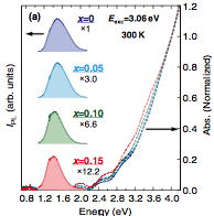
| The emission properties of Si1−xGex alloy nanocrystals (nc-Si1−xGex) in
an optical microcavity were studied, and the results were compared with
those of nc-Si in the same structure. The cavity consists of two distributed
Si/SiO2 Bragg reflectors (DBRs) sandwiching a thin SiO2 film containing
nc-Si1−xGex. The commonly observed cavity effects, that is, spectral narrowing,
high directionality, and photoluminescence (PL) enhancement in the normal
direction, were observed. In nc-Si1−xGex, PL lifetime was lengthened by
cavity formation, while that of nc-Si was shortened. This difference is
due to the different dielectric contrast between active layers and DBRs. |
|
| |
41. Kimiaki Toshikiyo, Masakazu Tokunaga, Shinji Takeoka, Minoru Fujii, and Shinji Hayashi,
"Electron Spin Resonance Study of Defects in Si1-xGex Alloy Nanocrystals Embedded in SiO2 Matrices; Mechanism of Luminescence Quenching,”
Journal of Applied Physics, Vol. 89, No. 9, 4917-4920, May (2001) |
| Dangling bond defects in Si1−xGex alloy nanocrystals (nc-Si1−xGex) as small
as 4 nm in diameter embedded in SiO2 thin films were studied by electron
spin resonance (ESR), and the effects of the defects on photoluminescence
(PL) properties were discussed. It was found that the ESR spectrum is a
superposition of signals from Si and Ge dangling bonds at the interfaces
between nc-Si1−xGex and SiO2 matrices (Si and Ge Pb centers). As the Ge
concentration increased, the signal from the Ge Pb centers increased, while
that from the Si Pb centers was nearly independent of Ge concentration.
The increase in the number of Ge Pb centers was accompanied by strong quenching
of the PL. The observed correlation between the two measurements suggests
that the Ge Pb centers act as efficient nonradiative recombination centers
for photogenerated carriers, resulting in the quenching of the main PL.
|
|
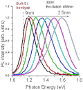 |
38. Shinji Takeoka, Minoru Fujii, and Shinji Hayashi,
"Size-dependent Photoluminescence from Surface-oxidized Si Nanocrystals in a Weak Confinement Regime,”
Physical Review B, Vol. 62, No. 24, pp. 16820 - 16825, December (2000). |
| Photoluminescence (PL) from surface-oxidized Si nanocrystals (nc-Si) was
studied as a function of the size. The size of nc-Si was comparable with
or larger than the Bohr radius of free excitons in bulk Si crystal (5 nm).
In contrast to smaller surface-oxidized nc-Si (typically as small as a
few nanometers in diameter), these relatively large nc-Si exhibited PL
properties with strong size dependence. A high-energy shift of the PL peak
from the vicinity of the bulk band gap to the visible region was observed.
This PL shift was accompanied by a shortening of the PL lifetime and an
increase in the exchange splitting energy of excitons. These size dependences
indicate that the PL originates from the recombination of excitons confined
in nc-Si. The differences in the PL properties between H-terminated and
surface-oxidized nc-Si are also discussed. |
|
| |
36. Minoru Fujii, Dmitri Kovalev, Joachim Diener, Frederick Koch, Shinji Takeoka, and Shinji Hayashi,
"Breakdown of the k-conservation Rule in Si1-xGex Alloy Nanocrystals: Resonant Photoluminescence Study,”
Journal of Applied Physics, Vol. 88, No. 10, pp. 5772 - 5776, November (2000). |
| Resonant photoluminescence from Si1 x Gex alloy nanocrystals as small
as 4 nm in diameter embedded in SiO2 thin film matrices was studied. In
pure Si nanocrystals, phonon structures were clearly observed, indicating
that optical transitions are assisted by momentum-conserving phonons. These
structures are quenched by adding a small amount of Ge atoms in Si nanocrystals,
i.e., due to the formation of Si1xGex alloy. Furthermore, the lifetime
of the radiative recombination became much faster in doped nanocrystals.
These results suggest that Si1xGex alloy formation leads to a disorder
in the translation invariance of the crystalline lattice, thus resulting
in the breakdown of the k-conservation rule. |
|
| |
32. Shinji Takeoka, Kimiaki Toshikiyo, Minoru Fujii, Shinji Hayashi, and Keiichi Yamamoto,
"Photoluminescence from Si1-xGex Alloy Nanocrystals,”
Physical Review B, Vol. 61, No. 23, pp. 15988-15992, June (2000). |
| Photoluminescence (PL) from Si1-xGex alloy nanocrystals (nc-Si1-xGex) as
small as 4–5 nm in diameter was studied as a function of the Ge content.
The nc-Si1-xGex samples were fabricated by the cosputtering of Si, Ge,
and SiO2 and postannealing at 1100°C. High-resolution transmission electron
microscopy, electron diffraction, and Raman spectroscopy clearly showed
the growth of spherical Si1-xGex nanocrystals in SiO2 matrices. The PL
spectra of nc-Si1-xGex were found to be very sensitive to the Ge content.
A low-energy shift of the PL peak from the widened band gap of Si nanocrystals
to that of Ge nanocrystals with increasing Ge content was clearly observed. |
|
| |
23. Shinji Takeoka, Minoru Fujii, Shinji Hayashi and Keiichi Yamamoto,
"Decay Dynamics of Near-infrared Photoluminescence from Ge Nanocrystals,”
Applied Physics Letters Vol. 74, No. 11, pp.1558-1560, March (1999). |
| Photoluminescence (PL) decay dynamics of Ge nanocrystals (nc-Ge) 1.2–3.2
nm in average diameter embedded in SiO2 matrices was studied. The samples
showed a PL peak in the near-infrared region with strong size dependence.
A very fast component (≪1 μs) was found in decay curves for all the samples.
For the samples containing relatively large nc-Ge, a slow component of
the order of microseconds was also observed. With decreasing the size,
the slow component gradually faded out, and the PL intensity increased
significantly. The transition from indirect to direct recombination of
carriers with decreasing the size is considered to be responsible for the
observed PL decay dynamics. |
|
| |
18. Shinji Takeoka, Minoru Fujii, Shinji Hayashi and Keiichi Yamamoto,
"Size-dependent Near-infrared Photoluminescence from Ge Nanocrystals Embedded in SiO2 Matrices,”
Physical Review B, Vol. 58, No. 12, pp. 7921 - 7925, September (1998).
|
| We have succeeded in observing the size dependent photoluminescence (PL)
from Ge nanocrystals (nc-Ge) with 0.9–5.3 nm in average diameter (dave)
in the near-infrared region. The nc-Ge were fabricated by rf cosputtering
of Ge and SiO2 and post annealing at 800°C. It was found that the sample
with dave=5.3nm shows a PL peak at about 0.88 eV. With decreasing the size,
the PL peak shifted to higher energies and reached 1.54 eV for the sample
with dave=0.9nm. It was also found that the PL intensity increases drastically
with decreasing the size. The observed strong size dependence of the PL
spectra indicates that the observed PL originates from the recombination
of electron-hole pairs confined in nc-Ge. |
|
| |
12. Yoshihiko Kanzawa, Takeshi Kageyama, Shinji Takeoka, Minoru Fujii,
Shinji Hayashi and Keiichi Yamamoto,
"Size-dependent Near-infrared Photoluminescence Spectra of Si Nanocrystals Embedded in SiO2 Matrices,”
Solid State Communications, Vol. 102, No. 7, pp. 533-537, May (1997).
|
| Photoluminescence (PL) spectra of Si nanocrystals embedded in SiO2 films
were measured as a function of the size. Samples were prepared by r.f.
cosputtering of Si and SiO2 and post-annealing. The average particle sizes
for all the samples were directly estimated by high-resolution transmission
electron microscopic observations. For each sample, a broad PL peak was
observed in the near-infrared region. As the average particle size decreased
from 3.8 nm to 2.7 nm, the peak exhibited a blue shift from 1.42 eV to
1.54 eV and its intensity increased progressively. This strong size dependence
of the PL peak suggests that the PL peak arises from the recombination
of electrons and holes confined in the Si nanocrystals. |
|
| |
2. Shinji Hayashi, Minoru Fujii, and Keiichi Yamamoto,
"Quantum Size Effects in Ge Microcrystals Embedded in SiO2 Thin Films,”
Japanese Journal of Applied Physics, Vol. 28, No. 8, pp. L1464-L1466, August (1989).
|
| By applying an rf co-sputtering technique, we have succeeded in producing
Ge microcrystals in SiO2 thin films for which direct characterization by
transmission electron microscopy is possible. As the size of the Ge microcrystals
decreased from 6.5 to 2.7 nm, the optical extinction (absorption) spectra
changed drastically. The structures corresponding to interband transitions
in bulk Ge disappeared, and the onset of extinction shifted to higher energies.
These spectral changes seem to arise from the three-dimensional confinement
of electrons and holes in the microcrystals. |
|
| |
| |
| |
|
|
|