| Book | Journal | Proceeding | Report | Memoir | Presentation |
| 2026 2025 2024 2023 2022 2021 2020 2019 2018 2017 2016 2015 2014 2013 2012 2011 2010 2009 2008 2007 2006 2005 2004 2003 2002 2001 2000 1999 1998 1997 1996 1995 1994 1993 1992 1991 1990 1989 1988 |
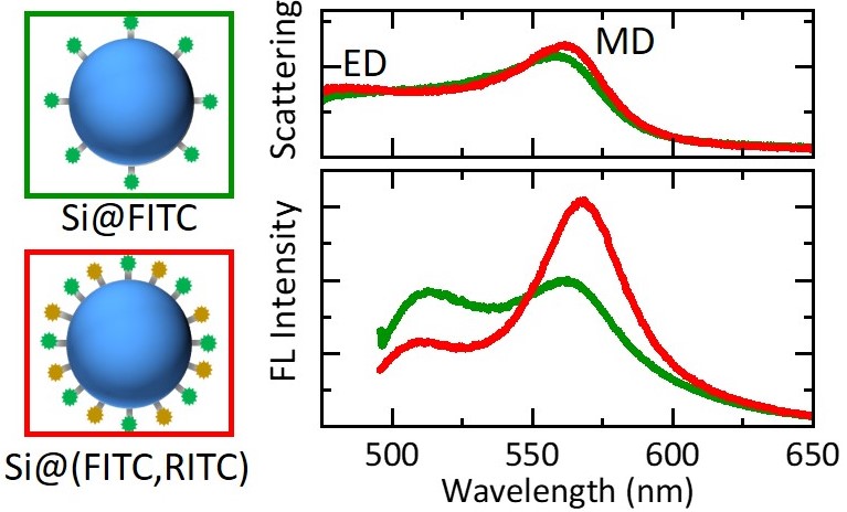
| 372. María Sanz-Paz, Nicole Siegel, Guillermo Serrera, Javier González-Colsa, Fangjia Zhu, Karol Kołątaj, Minoru Fujii, Hiroshi Sugimoto, Pablo Albella, Guillermo P. Acuna, "Color Routing and Beam Steering of Single-Molecule Emission with a Spherical Silicon Nanoantenna", Advanced Functional Materials, Vol. , Issue , pp.(2026). (First published:January 26, 2026) | |

|
Single-photon emitters radiate as electric dipoles, which limits light collection efficiency and complicates integration into flat photonic devices. Developing nanophotonic structures capable of directing photon emission with tunable angular distributions in the visible spectrum has been pursued for applications ranging from integrated optical systems to discrimination of molecular species. To date, such directional control has been achieved using components whose overall footprint is larger than the emission wavelength and often rely on lossy plasmonic components. Here, we employ the DNA origami technique for deterministic nanoscale assembly, positioning single fluorophores in nanometric proximity to a single silicon spherical nanoparticle (SiNP) and demonstrate unidirectional emission with forward-to-backward intensity ratios up to ∼7 dB. Furthermore, we show that a single silicon nanosphere antenna can function as a color router or a beam steerer depending on its size, emitter spectral range and emitter-nanoparticle distance, enabling the use of these structures as versatile functional components in photonic devices. |
| 371. Jiancheng Xu, Yuheng Mao, Yeshun Guo, Ruizhao Yao, Shulei Li, Hiroshi Sugimoto, Minoru Fujii, Fu Deng, Guangcan Li, and Sheng Lan, "Greatly enhanced photoluminescence of an integrated WSe₂ monolayer by exploiting the pure magnetic resonance and localized strain induced by a hybrid Si/Si₃N₄/Au nanoantenna", Optics Express, Vol. 34, Issue 2, pp.1369-1382 (2026). (First published: January 12, 2026) | |

|
Exploiting the optical resonances inherent to dielectric nanoparticles offers an effective approach for modulating light-matter interactions at the nanoscale while maintaining minimal optical losses. In this study, we introduce a hybrid nanoantenna platform composed of Si/Si3N4/Au layers, which facilitates the tuning of resonant multipolar modes and their application in enhancing the photoluminescence (PL) of WSe2 monolayer. By systematically varying the thickness of the Si3N4 spacer, we achieve modulation of both the spectral positions and spatial field distributions of the resonances associated with Si nanospheres, thereby enabling precise control over near-field confinement and far-field scattering characteristics. Optimal performance is observed with an 80 nm spacer thickness, where a distinct magnetic dipole resonance emerges near 750 nm. Additionally, fine-tuning the nanoparticle radius allows for controlled red- and blue-shifting of the resonant modes. These deliberately engineered resonances lead to a substantial enhancement of the PL emission from WSe2 integrated onto the hybrid structure, with an enhancement factor approximating 1609. The observed enhancement is attributed to a combination of intensified local electromagnetic fields and strain-induced exciton funneling, presenting a promising methodology for the active manipulation of light emission within integrated nanophotonic devices. |
| 370. Zheheng Song, Xi Lu, Oanh Vu, Jialu Song, Hiroshi Sugimoto, Minoru Fujii, Lars Berglund, Ilya Sychugov, "Selective Scatterers Improve Efficiency and Color Neutrality of Semitransparent Photovoltaics", ACS Photonics, Vol. 12, Issue 11, pp.6458-6467 (2025). (First published:November 6, 2025) | |||||||||||||||||||||||||||||||||||||||||||||||||||||||||||||||||||||||||||||||||||||||||||||||||||||||||||||||||||||||||||||||||||||||||||||||||||||||||||||||||||||||||||||||||||||||||||||||||||||||||||||||||||||||||||||||||||||||||||||||||||||||||||||||||||||||||||||||||||||||||||||||||||||||||||||||||||||||||||||||||||||||||||||||||||||||||||||||||||||||||||||||||||||||||||||||||||||||||||||||||||||||||||||||||||||||||||||||||||||||||||||||||||||||||||||||||||||||||||||||||||||||||||||||||||||||||||||||||||||||||||||||||||||||||||||||||||||||||||||||||||||||||||||||||||||||||||||||||||||||||||||||||||||||||||||||||||||||||||||||||||||||||||||||||||||||||||||||||||||||||||||||||||||||||||||||||||||||||||||||||||||||||||||||||||||||||||||||||||||||||||||||||||||||||||||||||||||||||||||||||||||||||||||||||

|
We demonstrate that dielectric Mie scatterers, in the form of silicon nanoparticles (SiNPs), can enhance both the performance and esthetics of semitransparent photovoltaic devices. Unlike plasmonic metal counterparts, dielectric SiNPs exhibit lossless, narrow-band, spectral, and spatially tunable scattering in the visible spectral range. Their effect on a luminescent solar concentrator (LSC) with high visible light transparency is analyzed both theoretically and experimentally as a model system. By selectively reflecting a specific spectral band, SiNPs increase the optical path length of solar photons within the active layer, leading to improved absorption and hence device efficiency. Simultaneously, this light management strategy ensures transmitted color neutrality, an important requirement for wider acceptance of semitransparent photovoltaics. Numerical simulations show that in the regime of individual SiNPs with diameters around 160 nm, a submonolayer surface coverage of ∼10% is sufficient to achieve color neutrality, at the same time enhancing photocurrent by 10–15% for an LSC device. Experimentally, such a dispersed SiNP layer on an LSC substrate is realized by depositing NPs with the surface capped by a sacrificial polymer shell. Subsequent etching of the shell by oxygen plasma leads to an LSC device with a functional selective scattering layer in line with theoretical predictions. | ||||||||||||||||||||||||||||||||||||||||||||||||||||||||||||||||||||||||||||||||||||||||||||||||||||||||||||||||||||||||||||||||||||||||||||||||||||||||||||||||||||||||||||||||||||||||||||||||||||||||||||||||||||||||||||||||||||||||||||||||||||||||||||||||||||||||||||||||||||||||||||||||||||||||||||||||||||||||||||||||||||||||||||||||||||||||||||||||||||||||||||||||||||||||||||||||||||||||||||||||||||||||||||||||||||||||||||||||||||||||||||||||||||||||||||||||||||||||||||||||||||||||||||||||||||||||||||||||||||||||||||||||||||||||||||||||||||||||||||||||||||||||||||||||||||||||||||||||||||||||||||||||||||||||||||||||||||||||||||||||||||||||||||||||||||||||||||||||||||||||||||||||||||||||||||||||||||||||||||||||||||||||||||||||||||||||||||||||||||||||||||||||||||||||||||||||||||||||||||||||||||||||||||||||
| 369. Saskia Fiedler, Loriane Monin, Hiroshi Sugimoto, Minoru Fujii, Wiebke Albrecht, Albert Polman, "Nanoscale Heat Flow and Thermometry in Laser-Heated Resonant Silicon Mie Nanospheres Probed with Spatially Resolved Cathodoluminescence Spectroscopy", ACS Photonics, Vol. 12, Issue 10, pp.5668-5674 (2025). (First published:September 19, 2025) | |||||||||||||||||||||||||||||||||||||||||||||||||||||||||||||||||||||||||||||||||||||||||||||||||||||||||||||||||||||||||||||||||||||||||||||||||||||||||||||||||||||||||||||||||||||||||||||||||||||||||||||||||||||||||||||||||||||||||||||||||||||||||||||||||||||||||||||||||||||||||||||||||||||||||||||||||||||||||||||||||||||||||||||||||||||||||||||||||||||||||||||||||||||||||||||||||||||||||||||||||||||||||||||||||||||||||||||||||||||||||||||||||||||||||||||||||||||||||||||||||||||||||||||||||||||||||||||||||||||||||||||||||||||||||||||||||||||||||||||||||||||||||||||||||||||||||||||||||||||||||||||||||||||||||||||||||||||||||||||||||||||||||||||||||||||||||||||||||||||||||||||||||||||||||||||||||||||||||||||||||||||||||||||||||||||||||||||||||||||||||||||||||||||||||||||||||||||||||||||||||||||||||||||

|
Many nanoscale technologies depend critically on precise knowledge and control of local temperature and heat flow, making robust nanothermometry essential for designing, optimizing, and ensuring the reliability of next-generation devices. In this work, we introduce a correlative method that combines laser excitation with scanning electron microscopy-based cathodoluminescence (SEM-CL) to probe photothermal effects in situ with nanoscale spatial resolution. We analyze the spatially resolved CL (30 keV) of resonant Mie modes in single silicon nanoparticles under continuous-wave laser irradiation (λ = 442 nm). The 235–250-nm-diameter crystalline nanospheres, placed on a Si3N4 membrane, show a strong electric quadrupole CL resonance of which the peak wavelength reversibly red-shifts upon laser-induced heating. A temperature of up to 585 ± 12 °C is derived from the spectral shifts for the highest laser power used (9.6 mW, ∼1 × 10⁶ W/cm2 at the substrate). Numerical heat flow simulations show that the measured steady-state temperatures are consistent with a geometry in which heat flow occurs through a contact area of up to 100 nm2, depending on laser power, between the Si nanosphere and the Si3N4 membrane. We postulate that this contact forms by reshaping of the particle–membrane geometry as it heats up in the initial phase of the laser irradiation, leading to an equilibrium geometry that results in the measured steady-state temperature. This work shows that CL of resonant nanostructures in combination with simulations can serve as sensitive probes of temperature and thermal conductivity. Spatially resolved CL nanothermometry in a SEM enables studies of nanoscale thermal properties of a wide range of device geometries such as electronic integrated circuits, surface catalysts, photovoltaic devices, and more. | ||||||||||||||||||||||||||||||||||||||||||||||||||||||||||||||||||||||||||||||||||||||||||||||||||||||||||||||||||||||||||||||||||||||||||||||||||||||||||||||||||||||||||||||||||||||||||||||||||||||||||||||||||||||||||||||||||||||||||||||||||||||||||||||||||||||||||||||||||||||||||||||||||||||||||||||||||||||||||||||||||||||||||||||||||||||||||||||||||||||||||||||||||||||||||||||||||||||||||||||||||||||||||||||||||||||||||||||||||||||||||||||||||||||||||||||||||||||||||||||||||||||||||||||||||||||||||||||||||||||||||||||||||||||||||||||||||||||||||||||||||||||||||||||||||||||||||||||||||||||||||||||||||||||||||||||||||||||||||||||||||||||||||||||||||||||||||||||||||||||||||||||||||||||||||||||||||||||||||||||||||||||||||||||||||||||||||||||||||||||||||||||||||||||||||||||||||||||||||||||||||||||||||||
| 368. Evelijn Akerboom, Hiroshi Sugimoto, Minoru Fujii, F. Javier García de Abajo, Albert Polman, "Angle-Resolved Cathodoluminescence Interferometry of Plasmonic and Dielectric Scatterers", Nano Letters, Vol. 25, Issue 39, pp. 14264–14269 (2025). (First published:September 18, 2025) | |||||||||||||||||||||||||||||||||||||||||||||||||||||||||||||||||||||||||||||||||||||||||||||||||||||||||||||||||||||||||||||||||||||||||||||||||||||||||||||||||||||||||||||||||||||||||||||||||||||||||||||||||||||||||||||||||||||||||||||||||||||||||||||||||||||||||||||||||||||||||||||||||||||||||||||||||||||||||||||||||||||||||||||||||||||||||||||||||||||||||||||||||||||||||||||||||||||||||||||||||||||||||||||||||||||||||||||||||||||||||||||||||||||||||||||||||||||||||||||||||||||||||||||||||||||||||||||||||||||||||||||||||||||||||||||||||||||||||||||||||||||||||||||||||||||||||||||||||||||||||||||||||||||||||||||||||||||||||||||||||||||||||||||||||||||||||||||||||||||||||||||||||||||||||||||||||||||||||||||||||||||||||||||||||||||||||||||||||||||||||||||||||||||||||||||||||||||||||||||||||||||||||

|
We demonstrate angle-resolved cathodoluminescence (CL) interferometry from electron-beam-excited plasmonic and dielectric nanostructures placed above a Au-coated substrate. We use 20–30 keV electrons to coherently excite plasmon-mediated radiation, which interferes with its mirror image, providing a method to determine the particle-substrate spacing. In an aloof excitation geometry, transition radiation emitted from the Au substrate adds to the interferogram and provides a means to probe the electron traveling time. The measured CL interferograms are in excellent agreement with a scattering and interferometry model in which a single electron coherently launches plasmons at two separate locations. Polarization-resolved CL measurements confirm the interferometric scattering model. Electron-excited Si Mie scatterers show interferograms modulated with resonantly enhanced emission. CL interferometry enables accurate measurement of critical distances in nanoscale geometries, in particular along the electron-beam direction, which are not easily accessible in electron microscopy, while offering a platform for studying optical interference in complex geometries. | ||||||||||||||||||||||||||||||||||||||||||||||||||||||||||||||||||||||||||||||||||||||||||||||||||||||||||||||||||||||||||||||||||||||||||||||||||||||||||||||||||||||||||||||||||||||||||||||||||||||||||||||||||||||||||||||||||||||||||||||||||||||||||||||||||||||||||||||||||||||||||||||||||||||||||||||||||||||||||||||||||||||||||||||||||||||||||||||||||||||||||||||||||||||||||||||||||||||||||||||||||||||||||||||||||||||||||||||||||||||||||||||||||||||||||||||||||||||||||||||||||||||||||||||||||||||||||||||||||||||||||||||||||||||||||||||||||||||||||||||||||||||||||||||||||||||||||||||||||||||||||||||||||||||||||||||||||||||||||||||||||||||||||||||||||||||||||||||||||||||||||||||||||||||||||||||||||||||||||||||||||||||||||||||||||||||||||||||||||||||||||||||||||||||||||||||||||||||||||||||||||||||||
| 367. Shintaro Kono, Oanh Vu, Mojtaba Karimi Habil, Hiroshi Sugimoto, Minoru Fujii, "Supraballs Composed of Mie-Resonant Silicon Nanospheres", Advanced Optical Materials, Vol.13, Issue 31, pp.e01846 (2025). (First published: September 19, 2025) | |||||||||||||||||||||||||||||||||||||||||||||||||||||||||||||||||||||||||||||||||||||||||||||||||||||||||||||||||||||||||||||||||||||||||||||||||||||||||||||||||||||||||||||||||||||||||||||||||||||||||||||||||||||||||||||||||||||||||||||||||||||||||||||||||||||||||||||||||||||||||||||||||||||||||||||||||||||||||||||||||||||||||||||||||||||||||||||||||||||||||||||||||||||||||||||||||||||||||||||||||||||||||||||||||||||||||||||||||||||||||||||||||||||||||||||||||||||||||||||||||||||||||||||||||||||||||||||||||||||||||||||||||||||||||||||||||||||||||||||||||||||||||||||||||||||||||||||||||||||||||||||||||||||||||||||||||||||||||||||||||||||||||||||||||||||||||||||||||||||||||||||||||||||||||||||||||||||||||||||||||||||||||||||||||||||||||||||||||||||||||||||||||||||||||||||||||||||||||||||||||||||

|
In this work, a supraball composed of high-refractive index (n~4) silicon nanoparticles (Si NSs) with diameters ranging from 100 to 200 nm having Mie-resonance in the visible range is fabricated via a solution-based self-assembly process. Structural characterization reveals the formation of highly spherical supraballs with diameters of 2 to 20 µm in which Si NSs are densely packed. Optical properties of individual supraballs made of different size Si NSs are systematically investigated. The main spectral feature of a densely packed supraball is well explained by a nanosphere-layer model. The effect of Si NS density, i.e., inter-NS distance, in a supraball on the optical response is studied by controlling the interparticle distance via two methods. Tuning the spacing between the NSs by oxidation reveals that the distance increase enhances the reflectance due to the appearance of the Mie resonance of individual Si NSs. The distance control by the formation of a thermoresponsive polymer shell on individual Si NSs in a supraball allows us to dynamically tune the interparticle distance through optically induced heating, and thus to dynamically control the reflectance spectrum. | ||||||||||||||||||||||||||||||||||||||||||||||||||||||||||||||||||||||||||||||||||||||||||||||||||||||||||||||||||||||||||||||||||||||||||||||||||||||||||||||||||||||||||||||||||||||||||||||||||||||||||||||||||||||||||||||||||||||||||||||||||||||||||||||||||||||||||||||||||||||||||||||||||||||||||||||||||||||||||||||||||||||||||||||||||||||||||||||||||||||||||||||||||||||||||||||||||||||||||||||||||||||||||||||||||||||||||||||||||||||||||||||||||||||||||||||||||||||||||||||||||||||||||||||||||||||||||||||||||||||||||||||||||||||||||||||||||||||||||||||||||||||||||||||||||||||||||||||||||||||||||||||||||||||||||||||||||||||||||||||||||||||||||||||||||||||||||||||||||||||||||||||||||||||||||||||||||||||||||||||||||||||||||||||||||||||||||||||||||||||||||||||||||||||||||||||||||||||||||||||||||||
| 366. Hiroaki Hasebe, Hiroshi Sugimoto, Minoru Fujii, "Kerker-Driven Janus Scattering in High Index Nanoparticle Metafluid for Naked-Eye Optical Encoding", ACS Applied Optical Materials, Vol. 3, Issue 9, pp.2078-2083 (2025). (First published:August 28, 2025) | |||||||||||||||||||||||||||||||||||||||||||||||||||||||||||||||||||||||||||||||||||||||||||||||||||||||||||||||||||||||||||||||||||||||||||||||||||||||||||||||||||||||||||||||||||||||||||||||||||||||||||||||||||||||||||||||||||||||||||||||||||||||||||||||||||||||||||||||||||||||||||||||||||||||||||||||||||||||||||||||||||||||||||||||||||||||||||||||||||||||||||||||||||||||||||||||||||||||||||||||||||||||||||||||||||||||||||||||||||||||||||||||||||||||||||||||||||||||||||||||||||||||||||||||||||||||||||||||||||||||||||||||||||||||||||||||||||||||||||||||||||||||||||||||||||||||||||||||||||||||||||||||||||||||||||||||||||||||||||||||||||||||||||||||||||||||||||||||||||||||||||||||||||||||||||||||||||||||||||||||||||||||||||||||||||||||||||||||||||||||||||||||||||||||||||||||||||||||||||||||||

|
Strong observation angle dependence of the scattering color is demonstrated in a metafluid in which size-purified silicon nanospheres are dispersed. Theoretical analyses based on Mie theory reveal that the observed macroscopic optical Janus property recognizable by naked eyes is induced by the Kerker effect of individual silicon nanospheres in a metafluid. Evaluation of the observation-angle dependent scattering spectra reveals that the angle dependent color change reaches ~80° in a hue circle. | ||||||||||||||||||||||||||||||||||||||||||||||||||||||||||||||||||||||||||||||||||||||||||||||||||||||||||||||||||||||||||||||||||||||||||||||||||||||||||||||||||||||||||||||||||||||||||||||||||||||||||||||||||||||||||||||||||||||||||||||||||||||||||||||||||||||||||||||||||||||||||||||||||||||||||||||||||||||||||||||||||||||||||||||||||||||||||||||||||||||||||||||||||||||||||||||||||||||||||||||||||||||||||||||||||||||||||||||||||||||||||||||||||||||||||||||||||||||||||||||||||||||||||||||||||||||||||||||||||||||||||||||||||||||||||||||||||||||||||||||||||||||||||||||||||||||||||||||||||||||||||||||||||||||||||||||||||||||||||||||||||||||||||||||||||||||||||||||||||||||||||||||||||||||||||||||||||||||||||||||||||||||||||||||||||||||||||||||||||||||||||||||||||||||||||||||||||||||||||||||||
| 365. Aleksandr Kostarev, Mohammad K. Abdosamadi, Hiroshi Sugimoto, Minoru Fujii, Anita Jannasch, Erik Schäffer, "Attonewton Force Resolution Measurements with Silicon Nanospheres at the Thermal Noise Limit in Ambient-Temperature Liquids", Nano Letters, Vol. 25, Issue 36, pp.13479-13481 (2025). (First published:August 5, 2025) | |||||||||||||||||||||||||||||||||||||||||||||||||||||||||||||||||||||||||||||||||||||||||||||||||||||||||||||||||||||||||||||||||||||||||||||||||||||||||||||||||||||||||||||||||||||||||||||||||||||||||||||||||||||||||||||||||||||||||||||||||||||||||||||||||||||||||||||||||||||||||||||||||||||||||||||||||||||||||||||||||||||||||||||||||||||||||||||||||||||||||||||||||||||||||||||||||||||||||||||||||||||||||||||||||||||||||||||||||||||||||||||||||||||||||||||||||||||||||||||||||||||||||||||||||||||||||||||||||||||||||||||||||||||||||||||||||||||||||||||||||||||||||||||||||||||||||||||||||||||||||||||||||||||||||||||||||||||||||||||||||||||||||||||||||||||||||||||||||||||||||||||||||||||||||||||||||||||||||||||||||||||||||||||||||||||||||||||||||||||||||||||||||||||||||||||||||||||||||||||

|
High-energy electron beams with energies in the 15–30 keV range are used to excite optical Mie modes in crystalline Si nanospheres with radius 80–100 nm. Cathodoluminescence (CL) spectra show emission from resonant electric and magnetic dipole and quadrupole modes, with relative intensities that depend strongly on electron energy and impact parameter. The measured trends are explained by a coupling model in which the electron-energy dependent CL excitation probability–and thus the CL emission–is proportional to the Fourier transform of the modal electric field at a spatial frequency determined by the electron velocity. As a result, the coupling to a specific resonant mode is strongly dependent on the electron energy and the impact parameter of the electron beam. This enables the selective enhancement of CL emission from a resonant mode by phase-matching with the electron velocity. A systematic study of spatial excitation probability for the electric dipole mode as a function of electron energy further confirms the validity of the coupling model. Angle-resolved cathodoluminescence measurements show strong directional emission due to far-field interference of coherently excited Mie modes. By varying the electron energy and impact parameter the intensity and interference of these modes can be controlled and the angular distribution tailored. The insights in the localized deep-subwavelength coherent excitation of resonant Mie modes explored here are important for studies in light-emitting nanostructures, sensors, and photovoltaics, in which the interplay of local modes and far-field directional emission must be controlled. | ||||||||||||||||||||||||||||||||||||||||||||||||||||||||||||||||||||||||||||||||||||||||||||||||||||||||||||||||||||||||||||||||||||||||||||||||||||||||||||||||||||||||||||||||||||||||||||||||||||||||||||||||||||||||||||||||||||||||||||||||||||||||||||||||||||||||||||||||||||||||||||||||||||||||||||||||||||||||||||||||||||||||||||||||||||||||||||||||||||||||||||||||||||||||||||||||||||||||||||||||||||||||||||||||||||||||||||||||||||||||||||||||||||||||||||||||||||||||||||||||||||||||||||||||||||||||||||||||||||||||||||||||||||||||||||||||||||||||||||||||||||||||||||||||||||||||||||||||||||||||||||||||||||||||||||||||||||||||||||||||||||||||||||||||||||||||||||||||||||||||||||||||||||||||||||||||||||||||||||||||||||||||||||||||||||||||||||||||||||||||||||||||||||||||||||||||||||||||||||
| 364. Yoshikazu Adachi, Izzah Machfuudzoh, Tetsuya Kubota, Sotatsu Yanagimoto, Hiroshi Sugimoto, Minoru Fujii, Takumi Sannomiya, "Temperature Measurement in Transmission Electron Microscope Using Cathodoluminescence of Whispering Gallery Mode", ACS Photonics, Vol. 12, Issue 8, pp.4737-4744 (2025). (First published: August 2, 2025) | |||||||||||||||||||||||||||||||||||||||||||||||||||||||||||||||||||||||||||||||||||||||||||||||||||||||||||||||||||||||||||||||||||||||||||||||||||||||||||||||||||||||||||||||||||||||||||||||||||||||||||||||||||||||||||||||||||||||||||||||||||||||||||||||||||||||||||||||||||||||||||||||||||||||||||||||||||||||||||||||||||||||||||||||||||||||||||||||||||||||||||||||||||||||||||||||||||||||||||||||||||||||||||||||||||||||||||||||||||||||||||||||||||||||||||||||||||||||||||||||||||||||||||||||||||||||||||||||||||||||||||||||||||||||||||||||||||||||||||||||||||||||||||||||||||||||||||||||||||||||||||||||||||||||||||||||||||||||||||||||||||||||||||||||||||||||||||||||||||||||||||||||||||||||||||||||||||||||||||||||||||||||||||||||||||||||||||||||||||||||||||||||||||||||||||||||||||||||||

|
We demonstrate a novel in situ temperature measurement technique in a transmission electron microscope (TEM) using cathodoluminescence (CL) of optical whispering gallery modes (WGMs) in silicon spheres. This method allows for non-invasive, high-resolution thermal analysis under various stimuli such as electron beam and laser irradiation. The temperature was monitored by the WGM spectral peak shifts of Si spheres of 300–600 nm in diameter. Under continuous electron beam and laser irradiation, we observed steady-state temperature increases In addition, the WGM spectral shifts under pulsed electron beams allowed us to extract temperature dynamics with microsecond resolution. These results show that WGM-based CL thermometry enables precise local temperature measurement and dynamic thermal response analysis within the TEM, offering new capabilities for in situ studies as well as the insights into the influence of the electron beam. | ||||||||||||||||||||||||||||||||||||||||||||||||||||||||||||||||||||||||||||||||||||||||||||||||||||||||||||||||||||||||||||||||||||||||||||||||||||||||||||||||||||||||||||||||||||||||||||||||||||||||||||||||||||||||||||||||||||||||||||||||||||||||||||||||||||||||||||||||||||||||||||||||||||||||||||||||||||||||||||||||||||||||||||||||||||||||||||||||||||||||||||||||||||||||||||||||||||||||||||||||||||||||||||||||||||||||||||||||||||||||||||||||||||||||||||||||||||||||||||||||||||||||||||||||||||||||||||||||||||||||||||||||||||||||||||||||||||||||||||||||||||||||||||||||||||||||||||||||||||||||||||||||||||||||||||||||||||||||||||||||||||||||||||||||||||||||||||||||||||||||||||||||||||||||||||||||||||||||||||||||||||||||||||||||||||||||||||||||||||||||||||||||||||||||||||||||||||||||
| 363. Théo Soler, Evelijn Akerboom, P. Elli Stamatopoulou, Hiroshi Sugimoto, Minoru Fujii, Saskia Fiedler, Albert Polman, "Electron-Energy Dependent Excitation and Directional Far-Field Radiation of Resonant Mie Modes in Single Si Nanospheres", ACS Photonics, Vol. 12, Issue 8, pp.4161-4170 (2025). (First published:July 24, 2025) | |||||||||||||||||||||||||||||||||||||||||||||||||||||||||||||||||||||||||||||||||||||||||||||||||||||||||||||||||||||||||||||||||||||||||||||||||||||||||||||||||||||||||||||||||||||||||||||||||||||||||||||||||||||||||||||||||||||||||||||||||||||||||||||||||||||||||||||||||||||||||||||||||||||||||||||||||||||||||||||||||||||||||||||||||||||||||||||||||||||||||||||||||||||||||||||||||||||||||||||||||||||||||||||||||||||||||||||||||||||||||||||||||||||||||||||||||||||||||||||||||||||||||||||||||||||||||||||||||||||||||||||||||||||||||||||||||||||||||||||||||||||||||||||||||||||||||||||||||||||||||||||||||||||||||||||||||||||||||||||||||||||||||||||||||||||||||||||||||||||||||||||||||||||||||||||||||||||||||||||||||||||||||||||||||||||||||||||||||||||||||||||||||||||||||||||||||||||

|
High-energy electron beams with energies in the 15–30 keV range are used to excite optical Mie modes in crystalline Si nanospheres with radius 80–100 nm. Cathodoluminescence (CL) spectra show emission from resonant electric and magnetic dipole and quadrupole modes, with relative intensities that depend strongly on electron energy and impact parameter. The measured trends are explained by a coupling model in which the electron-energy dependent CL excitation probability–and thus the CL emission–is proportional to the Fourier transform of the modal electric field at a spatial frequency determined by the electron velocity. As a result, the coupling to a specific resonant mode is strongly dependent on the electron energy and the impact parameter of the electron beam. This enables the selective enhancement of CL emission from a resonant mode by phase-matching with the electron velocity. A systematic study of spatial excitation probability for the electric dipole mode as a function of electron energy further confirms the validity of the coupling model. Angle-resolved cathodoluminescence measurements show strong directional emission due to far-field interference of coherently excited Mie modes. By varying the electron energy and impact parameter the intensity and interference of these modes can be controlled and the angular distribution tailored. The insights in the localized deep-subwavelength coherent excitation of resonant Mie modes explored here are important for studies in light-emitting nanostructures, sensors, and photovoltaics, in which the interplay of local modes and far-field directional emission must be controlled. | ||||||||||||||||||||||||||||||||||||||||||||||||||||||||||||||||||||||||||||||||||||||||||||||||||||||||||||||||||||||||||||||||||||||||||||||||||||||||||||||||||||||||||||||||||||||||||||||||||||||||||||||||||||||||||||||||||||||||||||||||||||||||||||||||||||||||||||||||||||||||||||||||||||||||||||||||||||||||||||||||||||||||||||||||||||||||||||||||||||||||||||||||||||||||||||||||||||||||||||||||||||||||||||||||||||||||||||||||||||||||||||||||||||||||||||||||||||||||||||||||||||||||||||||||||||||||||||||||||||||||||||||||||||||||||||||||||||||||||||||||||||||||||||||||||||||||||||||||||||||||||||||||||||||||||||||||||||||||||||||||||||||||||||||||||||||||||||||||||||||||||||||||||||||||||||||||||||||||||||||||||||||||||||||||||||||||||||||||||||||||||||||||||||||||||||||||||||
| 362. Nicole Siegel, María Sanz-Paz, Javier González-Colsa, Guillermo Serrera, Fangjia Zhu, Alan M. Szalai, Karol Kołątaj, Minoru Fujii, Hiroshi Sugimoto, Pablo Albella, Guillermo P. Acuna, "Distance-Dependent Interaction between a Single Emitter and a Single Dielectric Nanoparticle Using DNA Origami", Small Structures, Vol.6, Issue 11, pp.2500299 (2025). (First published: June 20, 2025) | |||||||||||||||||||||||||||||||||||||||||||||||||||||||||||||||||||||||||||||||||||||||||||||||||||||||||||||||||||||||||||||||||||||||||||||||||||||||||||||||||||||||||||||||||||||||||||||||||||||||||||||||||||||||||||||||||||||||||||||||||||||||||||||||||||||||||||||||||||||||||||||||||||||||||||||||||||||||||||||||||||||||||||||||||||||||||||||||||||||||||||||||||||||||||||||||||||||||||||||||||||||||||||||||||||||||||||||||||||||||||||||||||||||||||||||||||||||||||||||||||||||||||||||||||||||||||||||||||||||||||||||||||||||||||||||||||||||||||||||||||||||||||||||||||||||||||||||||||||||||||||||||||||||||||||||||||||||||||||||||||||||||||||||||||||||||||||||||||||||||||||||||||||||||||||||||||||||||||||||||||||||||||||||||||||||||||||||||||||||||||||||||||||||||||||||||||

|
Optical nanoantennas can manipulate light–matter interactions at the nanoscale, modifying the emission properties of nearby single photon emitters. To date, most optical antennas are based on metallic nanostructures that exhibit unmatched performance in terms of electric field enhancement but suffer from substantial ohmic losses that limit their applications. To circumvent these limitations, there is a growing interest in alternative materials. In particular, high-refractive-index dielectrics have emerged as promising candidates, offering negligible ohmic losses, and supporting both electric and magnetic resonances in the visible and near-infrared range that can unlock novel effects. Currently, the few available studies on dielectric nanoantennas focus on ensemble measurements. Here, the DNA origami technique is exploited to study the interaction between silicon nanoparticles and organic fluorophores at the single-molecule level, in controlled geometries and at different spectral ranges within the visible spectrum. Their distance-dependent interaction is characterized in terms of fluorescence intensity and lifetime, revealing a significant modification of the decay rate together with minimal quenching and a high-fluorescence quantum yield even at short distances from the dielectric nanoparticle. This work demonstrates the advantages of dielectric nanoantennas over their metallic counterparts and paves the way for their applications in single-molecule spectroscopy and sensing. | ||||||||||||||||||||||||||||||||||||||||||||||||||||||||||||||||||||||||||||||||||||||||||||||||||||||||||||||||||||||||||||||||||||||||||||||||||||||||||||||||||||||||||||||||||||||||||||||||||||||||||||||||||||||||||||||||||||||||||||||||||||||||||||||||||||||||||||||||||||||||||||||||||||||||||||||||||||||||||||||||||||||||||||||||||||||||||||||||||||||||||||||||||||||||||||||||||||||||||||||||||||||||||||||||||||||||||||||||||||||||||||||||||||||||||||||||||||||||||||||||||||||||||||||||||||||||||||||||||||||||||||||||||||||||||||||||||||||||||||||||||||||||||||||||||||||||||||||||||||||||||||||||||||||||||||||||||||||||||||||||||||||||||||||||||||||||||||||||||||||||||||||||||||||||||||||||||||||||||||||||||||||||||||||||||||||||||||||||||||||||||||||||||||||||||||||||
| 361. Oanh Vu, Jialu Song, Hiroshi Sugimoto, Minoru Fujii, "Polymer-Shell Coating of Mie-Resonant Silicon Nanospheres for Controlled Fabrication of Self-Assembled Monolayer", ACS Applied Nano Materias, Vol. 8, Issue 29, pp.14802-14810 (2025). (First published:July 16, 2025) | |||||||||||||||||||||||||||||||||||||||||||||||||||||||||||||||||||||||||||||||||||||||||||||||||||||||||||||||||||||||||||||||||||||||||||||||||||||||||||||||||||||||||||||||||||||||||||||||||||||||||||||||||||||||||||||||||||||||||||||||||||||||||||||||||||||||||||||||||||||||||||||||||||||||||||||||||||||||||||||||||||||||||||||||||||||||||||||||||||||||||||||||||||||||||||||||||||||||||||||||||||||||||||||||||||||||||||||||||||||||||||||||||||||||||||||||||||||||||||||||||||||||||||||||||||||||||||||||||||||||||||||||||||||||||||||||||||||||||||||||||||||||||||||||||||||||||||||||||||||||||||||||||||||||||||||||||||||||||||||||||||||||||||||||||||||||||||||||||||||||||||||||||||||||||||||||||||||||||||||||||||||||||||||||||||||||||||||||||||||||||||||||||||||||||||||

|
A polymer shell offers a unique opportunity to tailor the structural and optical properties of optically functional nanoparticles and their ensembles. Here, we develop a process to coat Mie-resonant silicon nanospheres (Si NSs) with a thermoresponsive poly(N-isopropylacrylamide) (PNIPAM) hydrogel shell. We show the formation of a PNIPAM shell of controlled thickness from the change of the hydrodynamic diameter and study the effect of thermoresponsive shrinkage and expansion of the shell on the Mie resonance of a Si NS. We then demonstrate that Si NSs with PNIPAM shells enable fabrication of cluster-free, self-assembled monolayers of Si NSs, in which distances between NSs are controlled by the PNIPAM shell thickness. | ||||||||||||||||||||||||||||||||||||||||||||||||||||||||||||||||||||||||||||||||||||||||||||||||||||||||||||||||||||||||||||||||||||||||||||||||||||||||||||||||||||||||||||||||||||||||||||||||||||||||||||||||||||||||||||||||||||||||||||||||||||||||||||||||||||||||||||||||||||||||||||||||||||||||||||||||||||||||||||||||||||||||||||||||||||||||||||||||||||||||||||||||||||||||||||||||||||||||||||||||||||||||||||||||||||||||||||||||||||||||||||||||||||||||||||||||||||||||||||||||||||||||||||||||||||||||||||||||||||||||||||||||||||||||||||||||||||||||||||||||||||||||||||||||||||||||||||||||||||||||||||||||||||||||||||||||||||||||||||||||||||||||||||||||||||||||||||||||||||||||||||||||||||||||||||||||||||||||||||||||||||||||||||||||||||||||||||||||||||||||||||||||||||||||||||
| 360. Yongan Hu, Patrick T. Probst, Mojtaba Karimi Habil, Hiroshi Sugimoto, Minoru Fujii, "Mechanically Tunable Optical Response in Silicon Nanosphere Metasurface Fabricated via Bottom-up Process", Advanced Optical Materials, Vol. 13, Issue 24, pp.01013 (2025). (First published: June 26, 2025) | |||||||||||||||||||||||||||||||||||||||||||||||||||||||||||||||||||||||||||||||||||||||||||||||||||||||||||||||||||||||||||||||||||||||||||||||||||||||||||||||||||||||||||||||||||||||||||||||||||||||||||||||||||||||||||||||||||||||||||||||||||||||||||||||||||||||||||||||||||||||||||||||||||||||||||||||||||||||||||||||||||||||||||||||||||||||||||||||||||||||||||||||||||||||||||||||||||||||||||||||||||||||||||||||||||||||||||||||||||||||||||||||||||||||||||||||||||||||||||||||||||||||||||||||||||||||||||||||||||||||||||||||||||||||||||||||||||||||||||||||||||||||||||||||||||||||||||||||||||||||||||||||||||||||||||||||||||||||||||||||||||||||||||||||||||||||||||||||||||||||||||||||||||||||||||||||||||||||||||||||||||||||||||||||||||||||||||||||||||||||||||||||||||||||||

|
Applications based on metasurfaces are often hampered by the limited scalability and real‐time tunability of lithographically produced samples (top‐down). Bottom‐up approaches that start from nanoparticle building blocks relax these constraints. Here, a large‐area mechano‐tunable metasurface composed of a square array of silicon nanospheres (Si NSs) is introduced. The metasurface is produced by capillarity‐assisted self‐assembly of size‐purified colloidal Si NSs that have Mie resonances in the visible and near‐infrared range. The collective response of Si NSs in the metasurface exhibits reflectance peaks originating from electric (ED) and magnetic dipole (MD) resonances of individual Si NSs. The resonance wavelengths are sensitive to the lattice constant and thus can be modulated in a wide wavelength range (≈130 nm) by external mechanical strain. At a proper strain level, the ED and MD lattice resonances spectrally overlap, resulting in destructive interference of the backward scattering light (lattice Kerker effect), which strongly suppresses the reflectance. The reflectance modulation is at a maximum of 45.9% and is reversible over 100 stretching‐releasing cycles. This suggests that the produced flexible metasurface can be a mechano‐tunable flexible optical component. | ||||||||||||||||||||||||||||||||||||||||||||||||||||||||||||||||||||||||||||||||||||||||||||||||||||||||||||||||||||||||||||||||||||||||||||||||||||||||||||||||||||||||||||||||||||||||||||||||||||||||||||||||||||||||||||||||||||||||||||||||||||||||||||||||||||||||||||||||||||||||||||||||||||||||||||||||||||||||||||||||||||||||||||||||||||||||||||||||||||||||||||||||||||||||||||||||||||||||||||||||||||||||||||||||||||||||||||||||||||||||||||||||||||||||||||||||||||||||||||||||||||||||||||||||||||||||||||||||||||||||||||||||||||||||||||||||||||||||||||||||||||||||||||||||||||||||||||||||||||||||||||||||||||||||||||||||||||||||||||||||||||||||||||||||||||||||||||||||||||||||||||||||||||||||||||||||||||||||||||||||||||||||||||||||||||||||||||||||||||||||||||||||||||||||
| 359. Moritz Junneman, Nicola Carlon Zambon, Hiroshi Sugimoto, Minoru Fujii, Lukas Novotny, Martin Frimmer, "Optical absorption of subwavelength silicon nanoparticles at telecom wavelengths", Physical Review B, Vol. 11, Issue 19, pp.195304 (2025). (First published: May 12, 2025) | |||||||||||||||||||||||||||||||||||||||||||||||||||||||||||||||||||||||||||||||||||||||||||||||||||||||||||||||||||||||||||||||||||||||||||||||||||||||||||||||||||||||||||||||||||||||||||||||||||||||||||||||||||||||||||||||||||||||||||||||||||||||||||||||||||||||||||||||||||||||||||||||||||||||||||||||||||||||||||||||||||||||||||||||||||||||||||||||||||||||||||||||||||||||||||||||||||||||||||||||||||||||||||||||||||||||||||||||||||||||||||||||||||||||||||||||||||||||||||||||||||||||||||||||||||||||||||||||||||||||||||||||||||||||||||||||||||||||||||||||||||||||||||||||||||||||||||||||||||||||||||||||||||||||||||||||||||||||||||||||||||||||||||||||||||||||||||||||||||||||||||||||||||||||||||||||||||||||||||||||||||||||||||||||||||||||||||||||||||||||||||||||||||||

|
We investigate the heating of silicon nanoparticles due to absorption of light at 1550 nm wavelength. We conclude that the strong temperature dependence of the absorption processes in silicon leads to a thermal runaway effect, destroying the particle once it reaches a critical temperature under intense irradiation. Our results bear relevance for recent proposals to use silicon particles for levitodynamics experiments. | ||||||||||||||||||||||||||||||||||||||||||||||||||||||||||||||||||||||||||||||||||||||||||||||||||||||||||||||||||||||||||||||||||||||||||||||||||||||||||||||||||||||||||||||||||||||||||||||||||||||||||||||||||||||||||||||||||||||||||||||||||||||||||||||||||||||||||||||||||||||||||||||||||||||||||||||||||||||||||||||||||||||||||||||||||||||||||||||||||||||||||||||||||||||||||||||||||||||||||||||||||||||||||||||||||||||||||||||||||||||||||||||||||||||||||||||||||||||||||||||||||||||||||||||||||||||||||||||||||||||||||||||||||||||||||||||||||||||||||||||||||||||||||||||||||||||||||||||||||||||||||||||||||||||||||||||||||||||||||||||||||||||||||||||||||||||||||||||||||||||||||||||||||||||||||||||||||||||||||||||||||||||||||||||||||||||||||||||||||||||||||||||||||||
| 358. Oanh Vu, Keisuke Ozawa, Mojtaba Karimi Habil, Hiroshi Sugimoto, Minoru Fujii, "Immobilization of Mie-Resonant Silicon Nanospheres on a Silica Substrate for Surface-Enhanced Fluorescence", Advanced Optical Materials, Vol. 13 , Issue 11, pp.2402808 (2025). (First published: March 22, 2025) | |||||||||||||||||||||||||||||||||||||||||||||||||||||||||||||||||||||||||||||||||||||||||||||||||||||||||||||||||||||||||||||||||||||||||||||||||||||||||||||||||||||||||||||||||||||||||||||||||||||||||||||||||||||||||||||||||||||||||||||||||||||||||||||||||||||||||||||||||||||||||||||||||||||||||||||||||||||||||||||||||||||||||||||||||||||||||||||||||||||||||||||||||||||||||||||||||||||||||||||||||||||||||||||||||||||||||||||||||||||||||||||||||||||||||||||||||||||||||||||||||||||||||||||||||||||||||||||||||||||||||||||||||||||||||||||||||||||||||||||||||||||||||||||||||||||||||||||||||||||||||||||||||||||||||||||||||||||||||||||||||||||||||||||||||||||||||||||||||||||||||||||||||||||||||||||||||||||||||||||||||||||||||||||||||||||||||||||||||||||||||||||||||

|
A process to immobilize Mie-resonant silicon nanospheres (Si NSs) on a large area substrate is developed for the application of surface-enhanced fluorescence (SEF) biosensors. The surface of size-purified Si NSs having the low-order Mie resonances in the visible to near-infrared range is functionalized with the epoxy group, and the Si NSs are immobilized on the surface of an amino-terminated silica (SiO2) substrate 1 × 1 cm2 in size by a fully wet process. The produced substrate exhibits a clear Mie resonant color. The wavelength of the reflectance maximum is controlled by the size of Si NSs, and the highest reflectance value reaches over 40%. In order to study the capability of the developed substrate as an SEF substrate, Lucifer Yellow CH dipotassium salt dye (LY) molecules are directly placed on the substrate and the photoluminescence (PL) properties are studied. The PL intensity is enhanced ≈14-fold on a substrate on which Si NSs 129 nm in average diameters are immobilized. Theoretical calculations by taking into account the size distribution of Si NSs explain the observed size dependence of the enhancement factor. | ||||||||||||||||||||||||||||||||||||||||||||||||||||||||||||||||||||||||||||||||||||||||||||||||||||||||||||||||||||||||||||||||||||||||||||||||||||||||||||||||||||||||||||||||||||||||||||||||||||||||||||||||||||||||||||||||||||||||||||||||||||||||||||||||||||||||||||||||||||||||||||||||||||||||||||||||||||||||||||||||||||||||||||||||||||||||||||||||||||||||||||||||||||||||||||||||||||||||||||||||||||||||||||||||||||||||||||||||||||||||||||||||||||||||||||||||||||||||||||||||||||||||||||||||||||||||||||||||||||||||||||||||||||||||||||||||||||||||||||||||||||||||||||||||||||||||||||||||||||||||||||||||||||||||||||||||||||||||||||||||||||||||||||||||||||||||||||||||||||||||||||||||||||||||||||||||||||||||||||||||||||||||||||||||||||||||||||||||||||||||||||||||
| 357. Keisuke Moriasa, Hiroaki Hasebe, Hiroshi Sugimoto, Minoru Fujii, "Sub-Bandgap Photocurrent Enhancement in Silicon Nanodisk Hexagonal Array Induced by FabryPerot Bound States in the Continuum", ACS Photonics, Vol. 12, Issue 3, pp.1658-1665 (2025). (First published: February 26, 2025) | |||||||||||||||||||||||||||||||||||||||||||||||||||||||||||||||||||||||||||||||||||||||||||||||||||||||||||||||||||||||||||||||||||||||||||||||||||||||||||||||||||||||||||||||||||||||||||||||||||||||||||||||||||||||||||||||||||||||||||||||||||||||||||||||||||||||||||||||||||||||||||||||||||||||||||||||||||||||||||||||||||||||||||||||||||||||||||||||||||||||||||||||||||||||||||||||||||||||||||||||||||||||||||||||||||||||||||||||||||||||||||||||||||||||||||||||||||||||||||||||||||||||||||||||||||||||||||||||||||||||||||||||||||||||||||||||||||||||||||||||||||||||||||||||||||||||||||||||||||||||||||||||||||||||||||||||||||||||||||||||||||||||||||||||||||||||||||||||||||||||||||||||||||||||||||||||||||||||||||||||||||||||||||||||||||||||||||||||||||||||||||||

|
We develop a silicon (Si) nanodisk array on a gold (Au) mirror structure as a platform for a Si-based narrow-band photodetector operating in the sub-bandgap wavelength range. Numerical simulations reveal that the structure possesses the Fabry–Pérot bound states in the continuum (BIC) arising from the destructive interference between the toroidal dipole resonance of the nanodisk array and the mirror dipole. At the critical coupling conditions, narrow band perfect absorption is achieved even if the extinction coefficient of Si nanodisks is very small. We produce the designed structure by nanosphere lithography and studied the reflectance and photocurrent spectra as a function of the distance between a Si nanodisk array and a Au mirror. We demonstrated that the photocurrent can be enhanced in the sub-bandgap wavelength range at the critical coupling condition, and the enhancement factor is modulated by the Si nanodisk array–mirror distance. | ||||||||||||||||||||||||||||||||||||||||||||||||||||||||||||||||||||||||||||||||||||||||||||||||||||||||||||||||||||||||||||||||||||||||||||||||||||||||||||||||||||||||||||||||||||||||||||||||||||||||||||||||||||||||||||||||||||||||||||||||||||||||||||||||||||||||||||||||||||||||||||||||||||||||||||||||||||||||||||||||||||||||||||||||||||||||||||||||||||||||||||||||||||||||||||||||||||||||||||||||||||||||||||||||||||||||||||||||||||||||||||||||||||||||||||||||||||||||||||||||||||||||||||||||||||||||||||||||||||||||||||||||||||||||||||||||||||||||||||||||||||||||||||||||||||||||||||||||||||||||||||||||||||||||||||||||||||||||||||||||||||||||||||||||||||||||||||||||||||||||||||||||||||||||||||||||||||||||||||||||||||||||||||||||||||||||||||||||||||||||||||
| 356. Nina Kudou, Taigo Morioka, Hiroshi Sugimoto, Minoru Fujii, Taniyuki Furuyama, "Bottom-up synthesis of seco-porphyrazines and their near-infrared optical properties", Journal of Porphyrins and Phthalocyanines, Vol. 29, Issue 03n04, pp.346-353 (2025). (First published: February 15, 2025) | |||||||||||||||||||||||||||||||||||||||||||||||||||||||||||||||||||||||||||||||||||||||||||||||||||||||||||||||||||||||||||||||||||||||||||||||||||||||||||||||||||||||||||||||||||||||||||||||||||||||||||||||||||||||||||||||||||||||||||||||||||||||||||||||||||||||||||||||||||||||||||||||||||||||||||||||||||||||||||||||||||||||||||||||||||||||||||||||||||||||||||||||||||||||||||||||||||||||||||||||||||||||||||||||||||||||||||||||||||||||||||||||||||||||||||||||||||||||||||||||||||||||||||||||||||||||||||||||||||||||||||||||||||||||||||||||||||||||||||||||||||||||||||||||||||||||||||||||||||||||||||||||||||||||||||||||||||||||||||||||||||||||||||||||||||||||||||||||||||||||||||||||||||||||||||||||||||||||||||||||||||||||||||||||||||||||||||||||||||||||||

|
Reducing the number of synthetic routes is critical for advancing the development of functional dyes and pigments. Herein, we present a novel one-step method for synthesizing secoporphyrazine skeletons, which are a class of 18π aromatic porphyrinoids. This bottom-up approach utilizes 1,3-diiminoisoindoline, benzonitrile derivatives, and palladium salts for ring construction. The resulting seco-porphyrazines contain unique twisted moieties, which are difficult to achieve with conventional methods. The absorption spectra reveal a split Q-band due to the asymmetric skeleton, indicating a strong interaction with near-infrared (NIR) light. In addition, molecular orbital calculations and electrochemical measurements support that skeletal asymmetry enhances NIR light utilization. | ||||||||||||||||||||||||||||||||||||||||||||||||||||||||||||||||||||||||||||||||||||||||||||||||||||||||||||||||||||||||||||||||||||||||||||||||||||||||||||||||||||||||||||||||||||||||||||||||||||||||||||||||||||||||||||||||||||||||||||||||||||||||||||||||||||||||||||||||||||||||||||||||||||||||||||||||||||||||||||||||||||||||||||||||||||||||||||||||||||||||||||||||||||||||||||||||||||||||||||||||||||||||||||||||||||||||||||||||||||||||||||||||||||||||||||||||||||||||||||||||||||||||||||||||||||||||||||||||||||||||||||||||||||||||||||||||||||||||||||||||||||||||||||||||||||||||||||||||||||||||||||||||||||||||||||||||||||||||||||||||||||||||||||||||||||||||||||||||||||||||||||||||||||||||||||||||||||||||||||||||||||||||||||||||||||||||||||||||||||||||
| 355. Keisuke Ozawa, Hiroshi Sugimoto, Daisuke Shima, Tatsuki Hinamoto, Mojtaba Karimi Habil, Yan Joe Lee, Søren Raza, Keisuke Imaeda, Kosei Ueno, Mark L. Brongersma, Minoru Fujii, "Routing Light Emission from Monolayer MoS2 by Mie Resonances of Crystalline Silicon Nanospheres", ACS Applied Optical Materials, Vol. 3, Issue 2, pp.375-382 (2025). (First published: February 15, 2025) | |

|
A dielectric Mie-resonant nanoantenna is capable of controlling the directionality of the emission from nearby quantum emitters through the excitation of multiple degenerate Mie resonances. A crystalline silicon nanosphere (Si NS) is a promising candidate for a dielectric nanoantenna because crystalline Si has a large refractive index (3.8 at 650 nm) and the small imaginary part of a complex refractive index (0.015 at 650 nm) as an optical material. In this work, we control the emission directionality of excitons supported by monolayer transition metal dichalcogenides (1L-TMDCs) using a Si NS. We first discuss the condition to extract the emission preferentially toward the Si NS side from the analytical calculations. We then study the photoluminescence (PL) of 1L-TMDCs on which differently sized single Si NSs are placed. We show that the PL spectral shape strongly depends on the emission direction, and that the emission toward the Si NS side (top) with respect to the opposite side (bottom) is the largest at a wavelength between the magnetic dipole and electric dipole Mie resonances of a Si NS. Finally, we quantitatively discuss the spectral shape of the top-to-bottom ratio from numerical simulations. |
| 354. Ruizhao Yao, Hiroshi Sugimoto, Tianhua Feng, Minoru Fujii, Shimei Liu, Xinming Li, Sheng Lan, Guang-Can Li, "Achieving Ideal Magnetic Light Emission with Electric-Type Emitters", Nano Letters, Vol. 24, Issue 42, pp.13315-13323 (2024). (First published: October 9, 2024) | |

|
Optical magnetic dipole (MD) emission predominantly relies on emitters with significant MD transitions, which, however, rarely exist in nature. Here, we propose a strategy to transform electric dipole (ED) emission to a magnetic one by elegantly coupling an ED emitter to a silicon nanoparticle exhibiting a strong MD resonance. This emission mode transformation enables an artificially ideal magnetic dipole source with an MD purity factor of up to 99%. The far-field emission patterns of such artificial MD sources were experimentally measured, which unambiguously resolved their magnetic-type emission origin. This study opens the path to achieving ideal magnetic dipole emission with nonmagnetic emitters, largely extending the availability of magnetic light emitters conventionally limited by nature. Beyond the fundamental significance in science, we anticipate that this study will also facilitate the development of magnetic optical nanosource and enable potential photonic applications relying on magnetic light emission. |
| 353. Kana Kondo, Mojtaba Karimi Habil, Kojiro Senda, Masato Adachi, Kenta Morita, Tatsuo Maruyama, Hiroshi Sugimoto, Minoru Fujii, "Size- and Wavelength-Selective Optical Heating in Mie-Resonant Silicon Nanospheres for Nanothermometry and Photothermal Applications", ACS Applied Nano Materials, Vol. 7, Issue 19, pp.23101-23110 (2024). (First published: September 30, 2024) | |

|
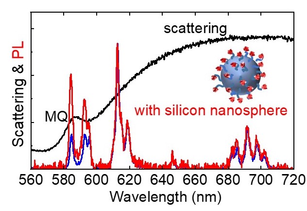
The photothermal heating properties of perfectly spherical crystalline silicon nanoparticles having the Mie resonances in the visible range are studied under different illumination wavelengths by using the Raman scattering peak as a nanothermometer. Analytical calculations reveal that the magnetic quadrupole (MQ) Mie mode is the most suitable mode for the photothermal heating. The experimentally obtained size and illumination wavelength dependence of the temperature rise agrees quantitatively with numerical simulations, and the heating efficiency reaches up to 381 K/(mW・µm2) when the illumination wavelength of 633 nm matches to the MQ resonance. Conversely, tuning the illumination wavelength to a relatively non-absorbing mode, such as the electric dipole (ED) mode, can significantly reduce the heating effect. In this context, the ED mode functions as a practically heating-less nanoantenna, promoting the surface-enhanced fluorescence of nearby dye molecules, while high-Q modes e.g., MQ and electric quadrupole (EQ) modes serve as an optical heating platform. Furthermore, the photothermal heating and the Raman thermometry of silicon nanoparticles in water and in cancer cells are demonstrated. |
| 352. Hao-Tse Su, Shao-Yuan Liu, Minoru Fujii, Hiroshi Sugimoto, Yoshito Y Tanaka , Teruki Sugiyama, "Optical trapping-induced crystallization promoted by gold and silicon nanoparticles", Photochemical & Photobiological Sciences, Vol. 23, pp.1697-1707 (2024). (First published: August 30, 2024) | |

|
This study investigates the promotion of sodium chlorate (NaClO3) crystallization through optical trapping, enhanced by the addition of gold nanoparticles (AuNPs) and silicon nanoparticles (SiNPs). Using a focused laser beam at the air–solution interface of a saturated NaClO3 solution with AuNPs or SiNPs, the aggregates of these particles were formed at the laser focus, the nucleation and growth of metastable NaClO3 (m-NaClO3) crystals were induced. Continued laser irradiation caused these m-NaClO3 crystals to undergo repeated cycles of growth and dissolution, eventually transitioning to a stable crystal form. Our comparative analysis showed that AuNPs, due to their significant heating due to higher photon absorption efficiency, caused more pronounced size fluctuations in m-NaClO3 crystals compared to the stable behavior observed with SiNPs. Interestingly, the maximum diameter of the m-NaClO3 crystals that appeared during the size fluctuation step was consistent, regardless of nanoparticle type, concentration, or size. The crystallization process was also promoted by using polystyrene nanoparticles, which have minimal heating and electric field enhancement, suggesting that the reduction in activation energy for nucleation at the particle surface is a key factor. These findings provide critical insights into the mechanisms of laser-induced crystallization, emphasizing the roles of plasmonic heating, particle surfaces, and optical forces. |
| 351. Shintaro Ogura, Hidemasa Negoro, Izzah Machfuudzoh, Zac Thollar, Tatsuki Hinamoto, F. Javier García de Abajo, Hiroshi Sugimoto, Minoru Fujii, Takumi Sannomiya, "Dielectric Sphere Oligomers as Optical Nanoantenna for Circularly Polarized Light", ACS Photonics, Vol. 11, Issue 8, pp.3323-3330 (2024). (First published: July 20, 2024) | |

|
Control of circularly polarized light (CPL) is important for next-generation optical communications as well as for investigating the optical properties of materials. In this study, we explore dielectric-sphere oligomers for chiral nanoantenna applications, leveraging the cathodoluminescence (CL) technique, which employs accelerated free electrons for excitation and allows mapping the optical response on the nanoscale. For a certain particle-dimers configuration, one of the spheres becomes responsible for the left-handed circular polarization of the emitted light, while right-handed circular polarization is selectively yielded when the other sphere is excited by the electron beam. Similar patterns are also observed in trimers. These phenomena are understood in terms of optical coupling between the electric and magnetic modes hosted by the dielectric spheres. Our research not only expands the understanding of CPL generation mechanisms in dielectric-sphere oligomer antennas but also underscores the potential of such structures in optical applications. We further highlight the utility of CL as a powerful analytical tool for investigating the optical properties of nanoscale structures as well as the potential of electron beams for light generation with switchable CPL parities. |
| 350. Jialu Song, Haruki Tanaka, Keisuke Moriasa, Hiroshi Sugimoto, Minoru Fujii, "Mie-Resonant Structural Color of Silicon Nanosphere Monolayer Coupled with Fabry–Pérot Cavity", ACS Applied Optical Materials, Vol. 2, Issue 7, pp.1420-1426 (2024). (First published: July 12, 2024) | |

|
Silicon (Si) nanospheres (NSs) 100-200 nm in diameter exhibit size-dependent scattering colors due to the Mie resonances. Because of the very high scattering efficiency, reflectance of ~50 % can be achieved in the monolayers, and thus ultra-thin and -lightweight color painting is possible with the Si NSs. In this work, we explore the possibility of controlling the color of Si NS monolayers by coupling with a Fabry–Pérot cavity for potential applications in dynamic color displays and environment sensors. First, scattering spectra of a single Si NS placed on a Si mirror via a silicon dioxide (SiO2) spacer are studied by numerical simulations for different spacer thicknesses. Similar simulations are then made for Si NS monolayers. The numerical results reveal that the reflected color can be tuned through the coupling strength of the spacer playing as a Fabry-Perot cavity and Mie resonances of Si NSs. Following the numerical results, Si NS monolayers are produced from the colloidal suspensions by the Langmuir-Blodgett method on surface-oxidized Si wafers, and the color control is experimentally demonstrated. |
| 349. Masato Adachi, Hiroshi Sugimoto, Kenta Morita, Tatsuo Maruyama, Minoru Fujii, "Scattering-Fluorescence Dual Mode Imaging in MnO2-Coated Silicon Nanospheres for Cancer Cell Detection", ACS Applied Materials & Interfaces, Vol. 16, Issue 26, pp.33963–33970 (2024). (First published: June 24, 2024) | |

|
A tumor micro-environment (TME)-responsive nanoprobe composed of a fluorescent dye-decorated silicon (Si) nanosphere core and a thin MnO2 shell is proposed for simple and intelligent detection of cancer cells. The Si nanosphere core with the diameters of 100-200 nm provides environment-independent Mie scattering imaging, while simultaneously, the MnO2 shell provides the capability to switch the on/off state of the dye fluorescence reacted to the glutathione (GSH) and/or H2O2 levels in a cancer cell. Si-MnO2 core-shell nanosphere probes are fabricated in a solution-based process from beforehand produced crystalline Si nanosphere cores. The fluorescence switching under exposure to GSH is demonstrated and the mechanism is discussed based on detailed optical characterizations including single particle spectroscopy. Different types of human cells are incubated with the nanoprobes and a proof of concept experiment is performed. From the combination of the robust scattering images and GSH- and H2O2-sensitive fluorescence images, feasibility of cancer cell detection by the multimodal nanoprobes is demonstrated. |
| 348. Nicole Siegel, Hiroaki Hasebe, Germán Chiarelli, Denis Garoli, Hiroshi Sugimoto, Minoru Fujii, Guillermo P. Acuna, Karol Kołątaj "Universal click-chemistry approach for the DNA functionalization of nanoparticles", Journal of American Chemical Society, Vol. 146, Issue 25, pp.17250–17260 (2024). (First published: June 13 2024) | |

|
Nanotechnology has revolutionized the fabrication of hybrid species with tailored functionalities. A milestone in this field is the DNA conjugation of nanoparticles, introduced almost 30 years ago, which typically exploits the affinity between thiol groups and metallic surfaces. Over the last decades, developments in colloidal research have enabled the synthesis of an assortment of non-metallic structures, such as high-index dielectric nanoparticles, with unique properties not previously accessible with traditional metallic nanoparticles. However, to stabilize, integrate and provide further functionality to non-metallic nanoparticles, reliable techniques for their functionalization with DNA will be crucial. Here, we combine wellestablished dibenzylcyclooctyne-azide clickchemistry with a simple freeze-thaw method to achieve the functionalization of silica and silicon nanoparticles, which form exceptionally stable colloids with a high DNA surface density of ⁓0.2 molecules/nm2. Furthermore, we demonstrate that these functionalized colloids can be selfassembled into high-index dielectric dimers with a yield over 50% via the use of DNA origami. Finally, we extend this method to functionalize other important nanomaterials, including oxides, polymers, core-shell and metal nanostructures. Our results indicate that the method presented herein serves as a crucial complement to conventional thiol functionalization chemistry and thus greatly expands the toolbox of DNA functionalized nanoparticles currently available. |
| 347. Hiroshi Sugimoto, Minoru Fujii, "Core/Shell Architecture Made from Mie-Resonant Silicon Nanoparticle: Design, Fabrication, and Photonic Applications", Chemical Physics Reviews, Vol. 5, Issue 2, pp.021304 (2024). (First published: 30 May 2024) | |

|
A silicon nanoparticle with a diameter of 100-300 nm possesses electric- and magnetic-type Mie resonances in the visible to near infrared ranges, and is recognized as a novel nanoplatform that can be used for light propagation control, light-matter interaction enhancement, structural coloration, bio-imaging and -sensing, etc. The functions of a silicon nanoparticle can be greatly extended by decorating the surface with various passive and active materials. In this mini-review, we introduce recent development of a core/shell architecture made from Mie resonant silicon nanoparticles. We start from state-of-the-art of the production of high-quality silicon nanoparticles. We then introduce fabrication processes of the core/shell architectures for a variety of shell materials that modify the properties of silicon nanoparticles and introduce new functions. The shell materials include passive low-refractive index materials, materials of tunable optical properties, fluorescence dyes, transition metal dichalcogenides, and noble metals with surface plasmon resonances. Finally, we will discuss our perspective for the development of future silicon-based core/shell architectures. |
| 346. Keisuke Ozawa, Masato Adachi, Hiroshi Sugimoto, Minoru Fujii, "Photoluminescence from FRET Pairs Coupled with Mie-Resonant Silicon Nanosphere", Nanoscale, Vol. 16, Issue 8, pp.4039-4046 (2024). (First published: 26 Jan 2024) | |
|
Optically resonant nanoparticles decorated with donor-acceptor molecular pairs have been attracting attentions for applications as nanoprobes in bioimaging and biosensing. We produce composite nanoparticles composed of donor-acceptor molecular pairs and silicon nanospheres (Si NSs) with diameters of 100-200 nm exhibiting Mie resonances in the visible range and study the effect of the Mie resonances on the photoluminescence properties. We show that the photoluminescence spectra are strongly modified by the Mie resonances, and the spectral shape is controlled in a wide range by the Si NS size; by controlling the size, we can bring the photoluminescence maximum from that of a donor molecule to that of an acceptor molecule almost continuously. From the photoluminescence decay properties in combination with theoretical calculations, we show that the observed strong modification of the spectral shape is mainly due to the Purcell effect to donor and acceptor molecules, and the effect of the Mie resonances to the Förster resonance energy transfer (FRET) rate is relatively small. We also show that because of the large Purcell effect and the small FRET rate enhancement, Mie resonances decrease the FRET efficiency. |
| 345. Jorge Olmos-Trigo, Hiroshi Sugimoto, Minoru Fujii, "Far-Field Detection of Near-Field Circular Dichroism Enhancements Induced by a Nanoantenna", Laser & Photonics Reviews, Vol. 18, Issue 5, pp.2300948 (2024). (First published: 20 January 2024) | |
|
Nanophotonics can enhance the inherent weak signal exhibited by chiral molecules in circular dichroism (CD) spectroscopy experiments. One mechanism to achieve this CD enhancement is based on increasing the optical chirality produced by nanophotonics antennas in their near-field, where chiral molecules are placed. However, ascertaining whether this CD enhancement is reached presents significant experimental challenges due to the complexity of measuring near-field optical chirality. Here, it is demonstrated that a local and single measurement of the degree of circular polarization in the far-field enables quantifying near-field CD enhancements. Thereby, based on this far-field measurement, the optimal response of the antenna is predicted for enhanced chiral sensing. Experimental validation of this near-to-far-field relation is provided for silicon spherical nanoantennas. The experimental results, supported by analytical theory and exact numerical simulations, can be interesting for the experimental characterization of devices capable of enhancing CD from a single far-field Stokes measurement. |
| 344. Haruki Tanaka, Shinnosuke Hotta, Tatsuki Hinamoto, Hiroshi Sugimoto, Minoru Fujii, "Monolayer of Mie-Resonant Silicon Nanospheres for Structural Coloration", ACS Applied Nano Materials, Vol. 7, Issue 3, pp.2605-2613 (2024). (First published: 29 January 2024) | |
|
Structural coloration of a monolayer of Mie-resonant silicon (Si) nanospheres (NSs) produced by a solution-based process is studied. It is shown by simulation that a monolayer of hexagonal close-packed Si NSs exhibits size-dependent structural color with the peak reflectance of ~50 %. The peak reflectance can be increased to over 90 % by introducing spaces between Si NSs. The high reflectance despite the small coverage is due to the very high scattering efficiency of Mie-resonant Si NSs. Monolayers of densely-packed Si NSs are produced from Si NS suspensions by the Langmuir-Blodgett (LB) method. The monolayers exhibit size-dependent structural color with the peak reflectance of 30-50 %. The color is very insensitive to the viewing angle, and the angle dependence of the reflectance spectra is very small. The peak reflectance is increased by increasing the distance between NSs by partially oxidizing the layers. The results demonstrate that iridescence-free structural coloration of a substance is possible by a layer of Si NSs much thinner than the monolayer, i.e., by sparsely scattered Si NSs. |
| 343. Hiroki Yoshikawa, Taiki Ueshima, Hiroshi Sugimoto, Jingchao Xu, Minoru Mizuhata, Minoru Fujii, "Single-Nanometer-Sized Boron and Phosphorus Co-Doped Silicon Nanoparticles for Negative Electrode of Lithium-Ion Batteries", ACS Applied Nano Materials, Vol. , Issue , pp. (2023). (First published: 11 December 2023) | |

|
A Si-based negative electrode for lithium-ion batteries (LIBs) is produced from methanol solutions of single-nanometer-size B and P co-doped Si nanoparticles (NPs) by drop-coating the solution on a substrate in air without using binders and conductive additives. Stable charge–discharge cycles are observed for films produced from Si NPs in the size range from less than 2 to 12.5 nm in diameter. It is shown that the performance and stability of the electrodes depend strongly on the size. The initial capacity increases with the size, while the stability decreases. The optimum diameter is ∼7 nm. In the electrode made from 7 nm diameter B and P co-doped Si NPs, the capacity is ∼3300 mAh/g and the Coulombic efficiency is ∼97% at a charge–discharge rate of 0.2C rate. |
| 342. Hidemasa Negoro, Hiroshi Sugimoto, Minoru Fujii, "Circularly Polarized Scattering Radiation From a Silicon Nanosphere", Advanced Optical Materials, Vol. 12, Issue 6, pp. 2301850 (2023). (First published: 18 October 2023) | |
|
A dielectric nanosphere with orthogonal electric dipole (ED) and magnetic dipole (MD) Mie resonances can be a nanoantenna radiating circularly polarized light in specific directions if the amplitudes and the phase relations are properly designed. First, theoretical calculations show that a silicon nanosphere illuminated with a linearly polarized plane wave radiates circularly polarized light at the wavelength in between the ED and MD resonances if the refractive index of a surrounding medium (nm) is ≈1.3; the ellipticity of the scattered light can be >0.99 when nm is in a 1.19–1.35 range. Size-purified silicon nanospheres suspended in water (nm = 1.33) are then prepared, and the angle- and circular-polarization-resolved scattering spectra are studied. It is experimentally demonstrated that circularly polarized light is radiated in specific directions under linearly polarized plane wave illumination. The results also show that the wavelength of the radiation of circularly polarized light can be controlled in the whole visible range by controlling the silicon nanosphere diameter in 100–200 nm range. |
| 341. Shinji Hayashi, Hiroshi Sugimoto, Minoru Fujii, Dmitry V. Nesterenko, Zouheir Sekkat, "Formation of Fano line shapes in optical responses and spectra of internal fields of excitonic nanospheres", Physical Review B, Vol. 108, Issue 12, pp. 125408 (2023). (First published: 8 September 2023) | |
|
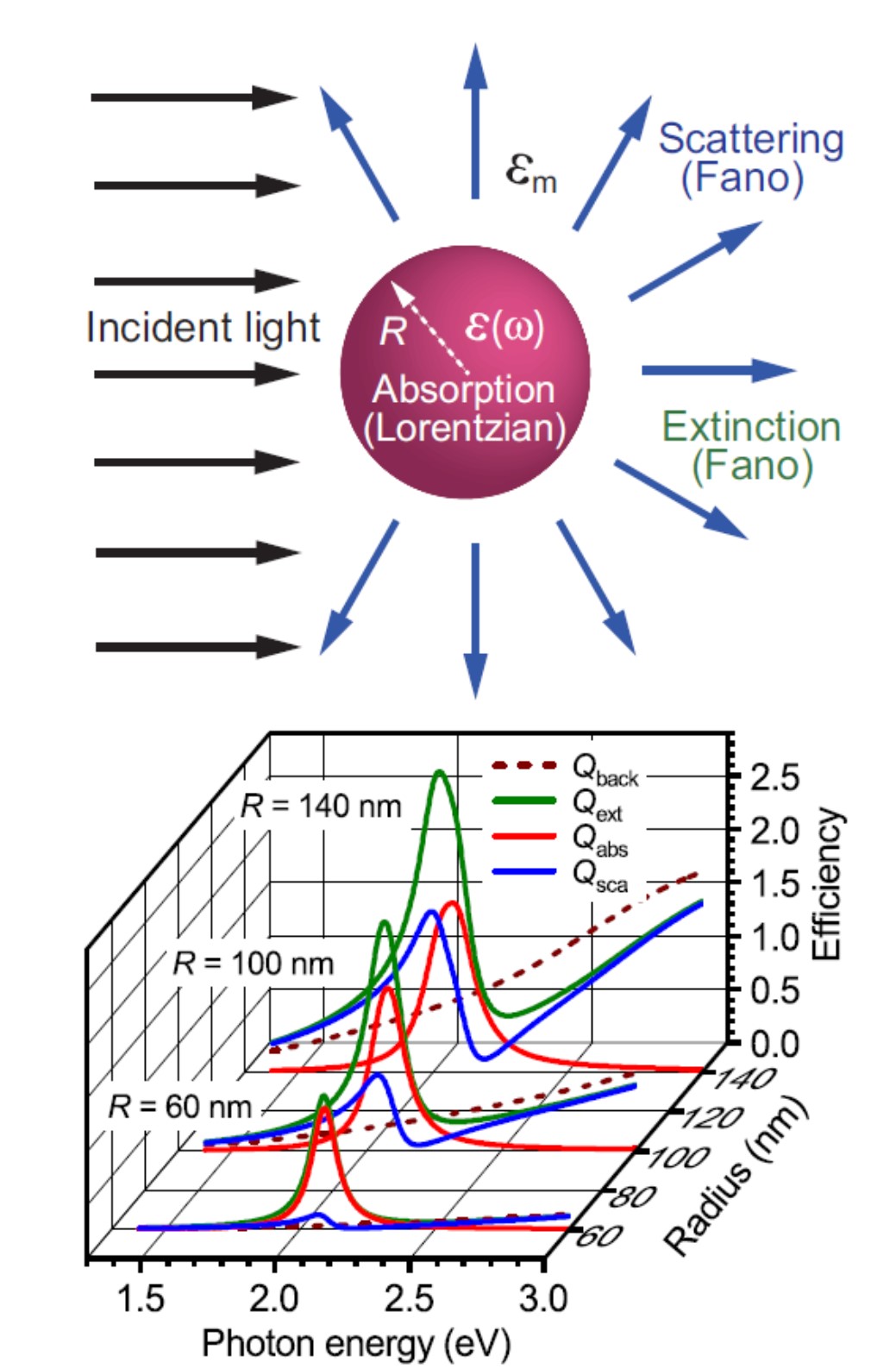
Dielectric nanoparticles not showing distinct Mie resonances have been discarded as useful elements of resonant nanophotonics. However, the incorporation of the excitonic transition into such nanoparticles may allow us to generate sharp resonances, in particular, Fano resonances, thereby enhancing the utility of such nanoparticles. In this work, on the basis of the Mie theory and its electrostatics approximation, we analyze analytically and numerically optical responses and resonant behaviors of internal fields in spherical excitonic nanoparticles. The excitonic sphere is characterized by a dielectric constant consisting of a background dielectric constant and a Lorentzian response of the exciton excitation. From equations of the electrostatics approximation, by appropriately accounting for the background scattering, it is shown analytically that the absorption efficiency is expressed as a Lorentzian function, while the efficiencies of the scattering and extinction are expressed in the form of the generalized Fano function (external Fano resonance). From the same procedures, it is also shown that the spectra of the enhancement factor of internal fields are described by the same generalized Fano function (internal Fano resonance). Equations appearing in the derivation clearly indicate that both the external and internal Fano resonances are caused by the interference between a nonresonant component and a resonant component, corresponding to a broad background and sharp excitonic transition, respectively. Assuming a model excitonic sphere that mimics a polymer sphere doped with J-aggregates of excitonic molecules, spectra of scattering, absorption and extinction efficiencies, as well as that of the enhancement factor of internal fields, are calculated including a size range beyond the small particle limit, for which the exact Mie theory is used. The generalized Fano functions are shown to reproduce very well the calculated spectra even beyond the small particle limit, provided that the sphere radius is less than an upper bound. The results of the present paper provide a firm basis for discussing the formation of the Fano line shapes in optical responses and spectra of internal fields of excitonic nanospheres. |
| 340. Hiroki Kasai, Hiroshi Sugimoto, Minoru Fujii, "Selective Enhancement of Crystal-Field-Split Narrow f-f Emission Lines of Europium Ions by Electric and Magnetic Purcell Effect of Mie Resonant Silicon Nanosphere", Advanced Optical Materials, Vol. 12, Issue 1, pp. 2301204 (2023). (First published: 2 August 2023) | |
|
Narrow-band Purcell enhancement for electric and magnetic dipole emitters by high-order Mie resonances up to the magnetic and electric octupole modes of a silicon nanosphere antenna is experimentally demonstrated. Eu3+ complexes are attached on the surface of a silicon nanosphere 160 to 316 nm in diameter, and the photoluminescence and scattering properties are investigated. It is shown that the branching ratio of the 5D0→7Fj (j = 0–4) f-f transitions of Eu3+ is controlled in a wide range by tuning the resonance wavelength of a silicon nanosphere by the size. Because of the high-quality factor resonances, not only a specific 5D0→7Fj transition, but also a specific Stark sublevel transition whose spectral separation is 3–9 nm can be selectively enhanced by precisely controlling the size of a silicon nanosphere with the accuracy of ≈2 nm. |
| 339. Hiroaki Hasebe, Hiroshi Sugimoto, Yoshino Katsurayama, Taniyuki Furuyama, Minoru Fujii, "Photosensitizing Metasurface Empowered by Enhanced Magnetic Field of Toroidal Dipole Resonance", Small, Vol. 19, Issue 42, pp.230519 (2023). (First published: 22 June 2023) | |
|
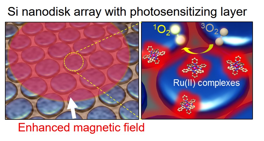
Photochemical reaction exploiting an excited triplet state (T1) of a molecule requires two steps for the excitation, i.e., electronic transition from the ground (S0) to singlet excited (S1) states and intersystem crossing to the T1 state. A dielectric metasurface coupled with photosensitizer that enables energy efficient photochemical reaction via the enhanced S0→T1 magnetic dipole transition is developed. In the direct S0→T1 transition, the photon energy of several hundreds of meV is saved compared to the conventional S0→ S1→T1 transition. To maximize the magnetic field intensity on the surface, a silicon (Si) nanodisk array metasurface with toroidal dipole resonances is designed. The surface of the metasurface is functionalized with ruthenium (Ru(II)) complexes that work as a photosensitizer for singlet oxygen generation. In the coupled system, the rate of the direct S0→T1 transition of Ru(II) complexes is 41-fold enhanced at the toroidal dipole resonance of a Si nanodisk array. The enhancement of a singlet oxygen generation rate is observed when the toroidal dipole resonance of a Si nanodisk array is matched with the direct S0→T1 transition wavelength of Ru(II) complexes. |
| 338. Akira Matsumori, Hiroshi Sugimoto, Minoru Fujii, "Unidirectional Transverse Light Scattering in Notched Silicon Nanosphere", Laser & Photonics Reviews, Vol. 17, Issue 8, pp.2300314 (2023). (First published: 1 June 2023) | |
|
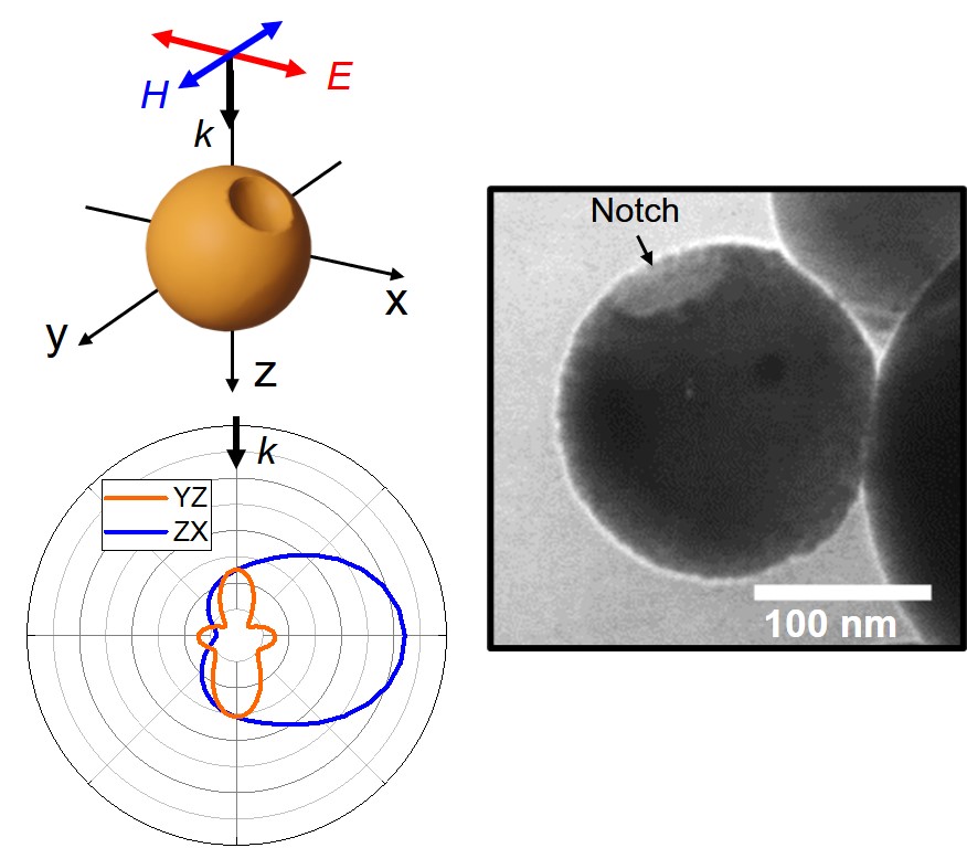
A nanoantenna that has the capability to direct light to a preferred direction is of paramount importance in a variety of applications in nanophotonics. Directional light scattering by a nanoantenna is achieved by properly controlling the interference between the electric and magnetic multipolar modes. In this work, it is theoretically and experimentally demonstrated that introduction of a small perturbation, i.e., a formation of a notch, to a Mie resonant silicon nanosphere (Si NS) results in the formation of a unique structure exhibiting unidirectional transverse light scattering in the visible range. Based on comprehensive numerical simulations including exact multipole decomposition analyses, the mechanism of the unidirectional transverse scattering is discussed. It is also shown that a notched Si NS can generate a relatively large transverse optical force as the recoil of the unidirectional transverse scattering. Finally, notched Si NSs are fabricated by a solution-based process. By combining incident-angle resolved single particle scattering spectroscopy with numerical simulations, directional transverse light scattering of a notched Si NS is confirmed. |
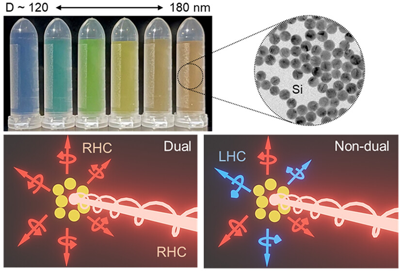
| 337. Hidemasa Negoro, Hiroshi Sugimoto, Minoru Fujii, "Helicity-Preserving Optical Metafluids", Nano Letters, Vol. 23, Issue 11, pp.5101-5107 (2023). (First published: 29 May 2023) | |
|
A colloidal suspension of photonic nanostructures exhibiting optical magnetism is dubbed an optical metafluid. A promising constituent of a metafluid is a nanosphere of high-refractive index dielectrics having the magnetic-type Mie resonances in the optical frequency. At the Kerker conditions, a dielectric nanosphere satisfies the electromagnetic duality symmetry condition and preserves the handedness of circularly polarized incident light. A metafluid of such dielectric nanospheres thus preserves the helicity of incident light. In the helicity-preserving metafluid, the local chiral fields around the constituent nanospheres are strongly enhanced, which improves the sensitivity of enantiomer-selective chiral molecular sensing. Here, we experimentally demonstrate that a solution of crystalline silicon nanospheres can be “dual” and “anti-dual” metafluids. We first theoretically address the electromagnetic duality symmetry of single silicon nanospheres. We then produce solutions of silicon nanospheres with narrow size distributions and experimentally demonstrate the “dual” and “anti-dual” behaviors. |
| 336. Keisuke Moriasa, Hiroaki Hasebe, Hiroshi Sugimoto, Minoru Fujii, "Bound States in the Continuum (BIC) in Silicon Nanodisk Array on Mirror Structure: Perfect Absorption Associated with Quasi-BIC below the Band Gap", Journal of Applied Physics, Vol. 133, Issue 17, pp.173102 (2023). (First published: 1 May 2023) | |
|
A structure composed of a hexagonal array of Si nanodisks having toroidal dipole resonances and a reflecting mirror separated by a SiO2 spacer is proposed as a platform that exhibits narrow band perfect absorption in the Si sub-band-gap wavelength range for CMOS compatible Si based photodetector operating below the band gap range. The numerical simulation reveals that the structure possesses Fabry-Pérot bound states in the continuum (FP-BIC) at proper spacer thicknesses due to the interference between toroidal dipole and its image dipole. By slightly detuning the spacer thickness to meet the critical coupling condition, narrow band perfect absorption appears despite the very small extinction coefficient assumed (5×10⁻⁴). The wavelength of the perfect absorption is controlled in a wide range by the structural parameters of a Si nanodisk hexagonal array and is insensitive to the fluctuation of the extinction coefficient and the choice of a metallic mirror. In the structure, over 90% of incident power can be absorbed in the Si region. This suggests that the structure can be used as a narrow band photodetector operating in the Si sub-band-gap wavelength range. We also evaluate the sensing performance of the proposed structure as an intensity based refractive index sensor operating in near infrared range. |
| 335. Daisuke Shima, Hiroshi Sugimoto, Artyom Assadillayev, Søren Raza, Minoru Fujii, "Gallium Phosphide Nanoparticles for Low-Loss Nanoantennas in Visible Range", Advanced Optical Materials, Vol. 11, Issue 12, pp.2203107 (2023). (First published: 22 March 2023) | |
|
|
Colloidal nanoparticles of gallium phosphide (GaP) with moderately high refractive index (n > 3) and a small extinction coefficient in the visible range are developed using a combination of mechanical milling and a pulsed laser melting process in solution. The combined process yields GaP nanoparticles with an almost spherical shape and the smooth surface. The single particle scattering spectroscopy reveals that smoothening of the surface by the pulsed laser melting process is crucial for achieving distinctive Mie resonances of the dipolar and higher-order modes in the visible range. The near field profile at the Mie resonances studied by electron energy loss spectroscopy in a scanning transmission electron microscope confirms the existence of the magnetic dipole mode. Finally, the Purcell enhancement of fluorescence of molecules on the surface due to the Mie resonances is demonstrated. |
| 334. Izzah Machfuudzoh, Tatsuki Hinamoto, F. Javier García de Abajo, Hiroshi Sugimoto, Minoru Fujii, and Takumi Sannomiya*, "Visualizing the Nanoscopic Field Distribution of Whispering-Gallery Modes in a Dielectric Sphere by Cathodoluminescence", ACS Photonics, Vol. 10, Issue 5, pp.1434-1445 (2023). (First published: 16 March 2023) | |
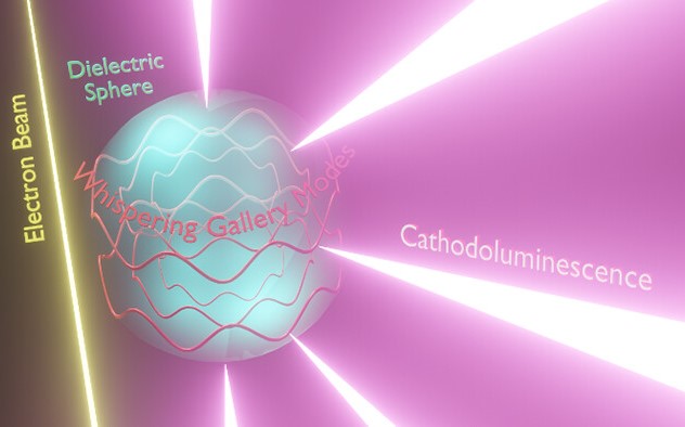
|
A spherical dielectric particle can sustain the so-called whispering-gallery modes (WGMs), which can be regarded as circulating electromagnetic waves, resulting in the spatial confinement of light inside the particle. Despite the wide adoption of optical WGMs as a major light confinement mechanism in salient practical applications, direct imaging of the mode fields is still lacking and only partially addressed by simple photography and simulation work. The present study comprehensively covers this research gap by demonstrating the nanoscale optical-field visualization of self-interference of light extracted from excited modes through experimentally obtained photon maps that directly portray the field distributions of the excited eigenmodes. To selectively choose the specific modes at a given light emission detection angle and resonance wavelength, we use cathodoluminescence-based scanning transmission electron microscopy supplemented with angle-, polarization-, and wavelength-resolved capabilities. Equipped with semi-analytical simulation tools, the internal field distributions of the whispering-gallery modes reveal that radiation emitted by a spherical resonator at a given resonance frequency is composed of the interference between multiple modes, with one or more of them being comparatively dominant, leading to a resulting distribution featuring complex patterns that explicitly depend on the detection angle and polarization. Direct visualization of the internal fields inside resonators enables a comprehensive understanding of WGMs that can shed light on the design of nanophotonic applications. |
| 333. Tadasha Jena, Md Tarik Hossain, Upasana Nath, Manabendra Sarma, Hiroshi Sugimoto, Minoru Fujii, and P. K. Giri, "Evidence for intrinsic defects and nanopores as hotspots in 2D PdSe2 dendrites for plasmon-free SERS substrate with a high enhancement factor", npj 2D materials and applications, Vol. 7, Article number 8 (2023). (First published: 23 February 2023) | |
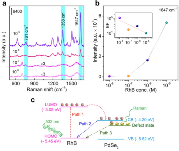
|
Surface-enhanced Raman spectroscopy (SERS), a very powerful tool for the identification of molecular species, has relied mostly on noble metal-based substrates to obtain a high enhancement factor. In this work, we demonstrate that self-driven intrinsic defects in 2D palladium di-selenide (PdSe2) dendrites grown at low temperature (280 °C) act as hotspots for high SERS enhancement. We grow 2D dendritic PdSe2 with ample intrinsic defects to exploit it for SERS application. X-ray electron spectroscopy (XPS) analysis reveals 9.3% outer layer and 4.7% interior Se vacancies. A detailed examination of atomic-scale defects revealed Se vacancy (VSe) coupled with Se–Pd–Se vacancy (VSe-Pd-Se) in monolayer PdSe2, and an array of line defects (Se vacancies) and nanopores in bilayer PdSe2 dendrites. Interestingly, our studies reveal that Se vacancy-rich PdSe2 gives rise to line defects that act like hotspots for SERS enhancement. Remarkably, the vacancy-rich dendritic PdSe2 shows a SERS enhancement factor >105 and can detect RhB at a concentration down to 10−8 M. We speculate that the topological line defects and the edge construction in PdSe2 dendrites act as metallic wire or edge, which is partly responsible for the high enhancement in the SERS signal. The high SERS sensitivity is explained on the basis of multiple charge transfer processes combined with the predicted metal-like behavior of the defected 2D PdSe2. Our conclusions are fully supported by the density functional theory calculation of the electronic density of states of the defective bilayer (2L) PdSe2, which remarkably exhibits metallic character. Being a defect-enabled SERS substrate, dendritic 2D PdSe2 fills the gap between conventional plasmonic SERS substrate and plasmon-free SERS substrate. |
| 332. Masato Adachi, Hiroshi Sugimoto, Yuya Nishimura, Kenta Morita, Chiaki Ogino, Minoru Fujii, "Fluorophore-Decorated Mie Resonant Silicon Nanosphere for Scattering/Fluorescence Dual-Mode Imaging", Small, Vol. 19, Issue 14, pp. 2207318 (2023). (First published: 24 January 2023) | |
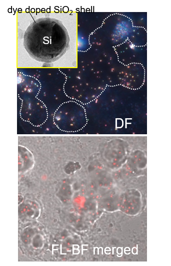
|
Inorganic nanoparticles with multiple functions have been attracting attention as multimodal nanoprobes in bioimaging, biomolecule detection, and medical diagnosis and treatment. A drawback of conventional metallic nanoparticle-based nanoprobes is the Ohmic losses that lead to fluorescence quenching of attached molecules and local heating under light irradiation. Here, metal-free nanoprobes capable of scattering/fluorescence dual-mode imaging are developed. The nanoprobes are composed of a silicon nanosphere core having efficient Mie scattering in the visible to near infrared range and a fluorophore doped silica shell. The dark-field scattering and photoluminescence images/spectra for nanoprobes made from different size silicon nanospheres and different kinds of fluorophores are studied by single particle spectroscopy. The fluorescence spectra are strongly modified by the Mie modes of a silicon nanosphere core. By comparing scattering and fluorescence spectra and calculated Purcell factors, the fluorescence enhancement factor is quantitatively discussed. In vitro scattering/fluorescence imaging studies on human cancer cells demonstrate that the developed nanoparticles work as scattering/fluorescence dual-mode imaging nanoprobes. |
| 331. Shinji Hayashi, Kengo Motokura, Minoru Fujii, Dmitry V. Nesterenko, Zouheir Sekkat, "Nested formation mechanisms of Fano line shape in far-field response of coupled waveguide multilayer structure revealed by analyses of local electric fields", Journal of Applied Physics, Vol. 132, Issue 16, pp.163104 (2022). (First published: 27 October 2022) | |
|
Based on electromagnetic calculations, the formation mechanism of the Fano line shape in the attenuated total reflection (far-field) spectrum of a coupled waveguide multilayer structure is studied in detail by tracing back to the behaviors of local electric fields. The Fano line shape of absorptance 𝐴 directly related to the reflectance by =1−𝐴 is shown to be generated by a superposition of a Fano line shape exhibited by local absorption in one of the waveguide layers and a Lorentzian line shape exhibited by local absorption in another waveguide layer. It is also shown that the Fano line shape of the first waveguide layer is generated by a superposition of different Fano line shapes exhibited by local electric fields at different positions inside the waveguide layer. These results unveil the nested mechanisms of the Fano line shape formation hidden in the behaviors of local electric fields. The Fano resonance inside the first waveguide layer is thought to be an example of the multiple Fano resonance arising from the interaction between multiple continua with a discrete state. |
| 330. Hiroaki Hasebe, Keisuke Moriasa, Kaito Yamashita, Hiroshi Sugimoto, Minoru Fujii, "Toroidal dipole-induced photocurrent enhancement in Si nanodisk hexagonal array below the band gap", ACS Photonics, Vol. 9, Issue 10, pp.3302-3309 (2022). (First published: 28 Sptember 2022) | |
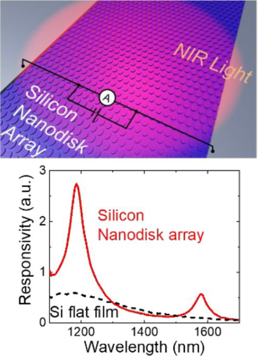
|
A hexagonal array of low-aspect-ratio silicon nanodisks is formed on a silicon thin film and the optical absorption and photocurrent properties are studied. Numerical simulations reveal that the nanodisk array possesses the toroidal dipole modes that tightly confine incoming light in a silicon region below the nanodisks. The field confinement brings about narrow-band absorption when the extinction coefficient (k) is very small, e.g., k =10-2~10-3. This suggests that defect-related sub-band gap absorption of silicon can be enhanced by utilizing the modes. Transmittance spectra of fabricated devices reveal that narrow dips assigned to the toroidal dipole resonances appear in the sub-band gap region. At the resonance wavelengths, the photocurrent is substantially enhanced; the enhancement factor reaches 30-fold. The observed narrow-band photodetection can be used as a current-detection-type refractive index sensor operating in the near infrared range. |
| 329. Hiroshi Sugimoto, Tatsuki Hinamoto, Yusuke Kazuoka, Artyom Assadillayev, Søren Raza, Minoru Fujii, "Mode Hybridization in Silicon Core-Gold Shell Nanosphere", Small, Vol. 18, Issue 45, pp.2204890 (2022). (First published: 26 September 2022) | |
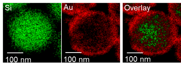
|
A dielectric core-metal shell nanosphere has attracted scientific and technological interests due to the unique optical resonances arising from the hybridization of surface plasmon modes and cavity modes. The previous studies focus on a low-index dielectric cire without its own optical resonances. Here, optical resonances of a core-shell nanosphere with a high refractive index (n~4) core with the lowest order Mie resonances in the visible range are investigated theoretically and experimentally. Scattering and absorption spectra of a core-shell nanosphere for different values of the core refractive index are first analyzed and there is a transition of the hybridization scheme around n ~ 2. Above the value, a characteristic hybridized mode with strong absorption and weak scattering emerges in the near-infrared range. A core-shell nanosphere composed of a silicon core and a gold shell is prepared and the resonance modes are studied by single particle scattering spectroscopy and electron energy loss spectroscopy (EELS) in a transmission electron microscope. The core-shell nanospheres exhibit the hybridized modes depending on the core diameter. The hybridized mode as well as the higher order one that is not observable in the scattering spectroscopy are observed in the EELS. |
| 328. Sumana Paul, Joydip Ghosh, Tarik Hossain, Hiroaki Hasebe, Hiroshi Sugimoto, Minoru Fujii, Pravat Giri, "Interfacial Charge Transfer Induced Enhanced Near-Infrared Photoluminescence and Enhanced Visible Photodetection in 2D/0D Bi2Se3/CsPbBr2I Heterojunction with Type-I Band Alignment", The Journal of Physical Chemistry C, Vol. 126, Issue 39, pp.16721-16731 (2022). (First published: 22 September 2022) | |
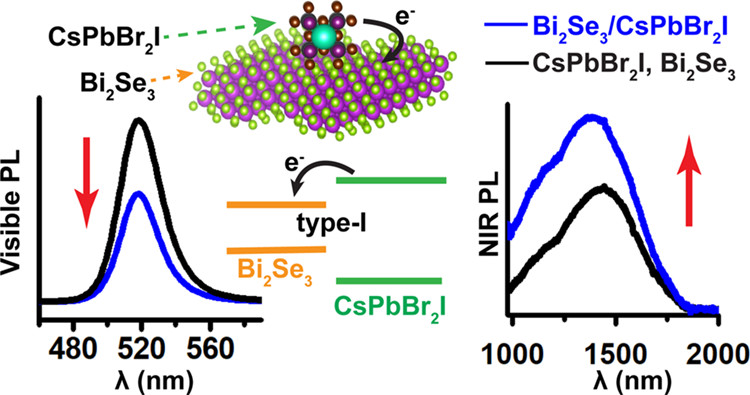
| Unraveling the charge transfer across a heterointerface is crucial for cutting-edge optoelectronic applications, including photodetectors, solar photovoltaics, light-emitting diodes, and so on. The incorporation of perovskite nanocrystals (NCs) into optoelectronics is limited primarily because of the presence of grain boundaries, carrier trapping, and ion migration, which restricts charge/energy transfer. Combining perovskite NCs with two-dimensional (2D) materials is a powerful approach to enhance energy harvesting and transport at the 0D-2D heterointerface. A simple sonication method was adopted to integrate zero-dimensional (0D) mixed halide perovskite CsPbBr2I NCs and topological 2D Bi2Se3 nanosheets (NSs) to realize a nanohybrid system. A series of optical signatures such as Raman shift, quenching of photoluminescence (PL), and shortened fluorescence lifetime in the nanohybrid clearly substantiate the interfacial charge transfer dynamics. Cyclic voltammetry and Kelvin probe force microscopy analysis and the optical studies established the type-I band alignment between perovskite NCs and Bi2Se3 NSs. The charge transfer dynamics of the nanohybrid was confirmed from the dramatic quenching of the PL intensity of CsPbBr2I NCs and an associated increase in the NIR PL as well as visible PL intensities of the Bi2Se3 NSs owing to increased carrier density caused by charge transfer. Furthermore, improved photoresponse performance of the hybrid system demonstrates the role of interfacial carrier transfer in 2D-0D nanohybrids, suppressing the radiative recombination in the light-harvesting perovskite NCs. The nanohybrid-based photodetector exhibits a high spectral responsivity of 14.4 A/W, a spectral detectivity of 0.4 × 10¹² Jones, and a fast growth/decay time of 82 μs/24 μs. These results will stimulate further exploration of topological 2D materials/halide perovskite-based novel hybrid functional devices for photodetection, light-harvesting, and light-emitting applications. |
| 327. Yinggang Wang, Hiroshi Sugimoto, Minoru Fujii, "Size-dependent Mutual Charge Transfer between B and P codoped Si Quantum Dots and Monolayer MoS2", The Journal of Physical Chemistry C, Vol. 126, Issue 38, pp.16401-16408 (2022). (First published: 19 September 2022) | |
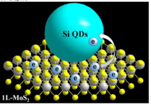
|
Heterostructures built from two-dimensional (2D) transition metal dichalcogenide (TMD) monolayers and quantum dots (0D) offer a large variety of systems for probing the fundamental physics and for the device applications. In this work, 2D/0D heterostructures comprised of monolayer MoS2 (1L-MoS2) and Si quantum dots (QDs) are produced and the mutual charge transfer is studied. It is shown that the charge transfer property depends strongly on the size of Si QDs. Decoration of a 1L-MoS2 flake with Si QDs 3.5 nm in diameter results in the quenching of the PL, while the decoration with Si QDs 9.0 nm in diameter enhances it. The results indicate that the direction of the charge transfer is different depending on the Si QD diameter. Contributions of the A excitons, B excitons, biexcitons and trions to total PL spectra are analyzed in a wide excitation power range and the mechanism of the charge transfer is discussed. |
| 326. Mark K. Svendsen, Hiroshi Sugimoto, Artyom Assadillayev, Daisuke Shima, Minoru Fujii, Kristian S. Thygesen, Søren Raza, "Computational Discovery and Experimental Demonstration of Boron Phosphide Ultraviolet Nanoresonators", Advanced Optical Materials, Vol. 10, Issue 16, pp.220422 (2022). (First published: 29 May 2022) | |
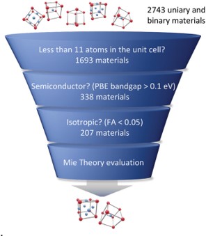
|
Controlling ultraviolet light at the nanoscale using optical Mie resonances holds great promise for a diverse set of applications, such as lithography, sterilization, and biospectroscopy. Access to the ultraviolet requires materials with a high refractive index and wide band gap energy. Here, the authors systematically search for such materials by computing the frequency-dependent optical permittivity of 338 binary semiconductors and insulators from first principles, and evaluate their scattering properties using Mie theory. This analysis reveals several interesting candidate materials among which boron phosphide (BP) appears most promising. Then BP nanoparticles are prepared and it is demonstrated that they support Mie resonances at visible and ultraviolet wavelengths using both far-field optical measurements and near-field electron energy-loss spectroscopy. A laser reshaping method is also presented to realize spherical Mie-resonant BP nanoparticles. With a refractive index over three and low absorption losses in a broad spectral range spanning from the infrared to the near ultraviolet, BP is an appealing material for a broad range of applications in dielectric nanophotonics. |
| 325. Hiroto Shinomiya, Hiroshi Sugimoto, Tatsuki Hinamoto, Yan Joe Lee, Mark L. Brongersma, Minoru Fujii, "Enhanced Light Emission from Monolayer MoS2 by Doubly Resonant Spherical Si Nanoantennas", ACS Photonics, Vol. 9, Issue 5, pp. 1741-1747 (2022). (First published: 19 April 2022) | |
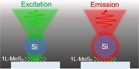
|
Optical antennas provide a powerful tool to control local photonic environments and enhance light emission from two-dimensional transition-metal dichalcogenides. Dielectric nanoantennas with multipolar Mie resonances bring unique advantages for achieving simultaneous enhancement of the absorption and emission processes. Here, we achieve a strong modification of the photoluminescence (PL) behavior of monolayer MoS2 by a spherical nanoparticle (NP) of crystalline silicon (Si) that works as a double resonance nanoantenna. From theoretical calculations for in-plane dipoles placed beneath a Si NP nanoantenna with different sizes, we explore optimal conditions for the double resonances. Then, we develop a heterostructure composed of a Si NP and a monolayer MoS2 sheet with a comparable diameter and investigate the scattering, PL, and PL excitation spectra across a wide Si NP size range. We show that the spectral shape is significantly modified and PL intensity is enhanced up to ?10-fold due to the coupling of the excitation process to the magnetic quadrupole resonance and the emission process to the magnetic dipole resonance |
| 324. Tatsuki Hinamoto, Yea-Shine Lee, Sina Abedini Dereshgi,Jennifer G. DiStefano, Roberto dos Reis, Hiroshi Sugimoto, Koray Aydin, Minoru Fujii,V inayak P. Dravid "Resonance Couplings in Si@MoS2 Core-Shell Architectures", Small, Vol. 18, Issue 17, pp.2200413 (2022). (First published: 19 March 2022) | |
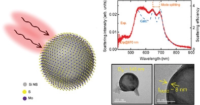
|
Heterostructures of transition metal dichalcogenides and optical cavities that can couple to each other are rising candidates for advanced quantum optics and electronics. This is due to their enhanced light-matter interactions in the visible to near-infrared range. Core-shell structures are particularly valuable for their maximized interfacial area. Here, the chemical vapor deposition synthesis of Si@MoS2 core-shells and extensive structural characterization are presented. Compared with traditional plasmonic cores, the silicon dielectric Mie resonator core offers low Ohmic losses and a wider spectrum of optical modes. The magnetic dipole (MD) mode of the silicon core efficiently couples with MoS2 through its large tangential component at the core surface. Using transmission electron microscopy and correlative single-particle scattering spectroscopy, MD mode splitting is experimentally demonstrated in this unique Si@MoS2 core-shell structure. This is evidence for resonance coupling, which is limited to theoretical proposals in this particular system. A coupling constant of 39 meV is achieved, which is ~1.5-fold higher than previous reports of particle-on-film geometries with a smaller interfacial area. Finally, higher-order systems with the potential to tune properties are demonstrated through a dimer system of Si@MoS2, forming the basis for emerging architectures for optoelectronic and nanophotonic applications. |
| 323. Saskia Fiedler, P. Elli Stamatopoulou, Artyom Assadillayev, Christian Wolff, Hiroshi Sugimoto, Minoru Fujii, N. Asger Mortensen, Soren Raza, and Christos Tserkezis, "Disentangling Cathodoluminescence Spectra in Nanophotonics: Particle Eigenmodes vs Transition Radiation", Nano Letters, Vol. 22, Issue 6, pp.2320-2327 (2022). (Published Online: 14 March 2022) | |
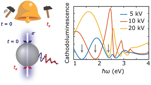
|
Cathodoluminescence spectroscopy performed in an electron microscope has proven a versatile tool for analyzing the near- and far-field optical response of plasmonic and dielectric nanostructures. Nevertheless, the transition radiation produced by electron impact is often disregarded in the interpretation of the spectra recorded from resonant nanoparticles. Here we show, experimentally and theoretically, that transition radiation can by itself generate distinct resonances that, depending on the time-of-flight of the electron beam inside the particle, can result from constructive or destructive interference in time. Superimposed on the eigenmodes of the investigated structures, these resonances can distort the recorded spectrum and lead to potentially erroneous assignment of modal characters to the spectral features. We develop an intuitive analogy that helps distinguish between the two contributions. As an example, we focus on the case of silicon nanospheres and show that our analysis facilitates the unambiguous interpretation of experimental measurements on Mie-resonant nanoparticles. |
| 322. Akira Matsumori, Hiroshi Sugimoto, and Minoru Fujii, "Silicon Nanosphere with Accessible Magnetic Hotspot", Advanced Optical Materials, Vol. 10, Issue 8, pp.2102574 (2022). (Published Online: 28 February 2022) | |
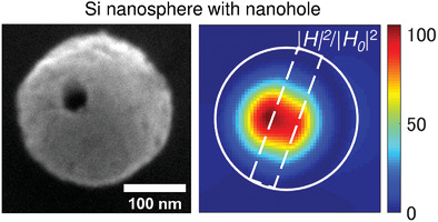
|
High refractive index dielectric nanoparticles supporting the magnetic dipole (MD) Mie resonance are capable of inducing strongly enhanced magnetic field at an optical frequency, and have great potential for enhancing light?matter interactions such as magnetic dipole transitions of ions and molecules. However, the magnetic hotspot is usually located inside a nanoparticle and thus the development of technology to access the hotspot remains an urgent issue. Here, a silicon (Si) nanosphere having an access hole to the magnetic hotspot is proposed. Numerical simulations for a Si nanosphere with a hole of different diameters and depths are performed. Then, a solution-based process to dig an access hole to a Si nanosphere is developed. A spectroscopic method to analyze nanohole-induced anisotropy of a spherical nanoantenna is also developed. Finally, in combination with numerical simulations and angle-resolved scattering measurements of a Si nanosphere with a nanohole, it is shown that the magnetic field intensity is 100-fold enhanced at the nanohole. |
| 321. Hidemasa Negoro, Hiroshi Sugimoto, Tatsuki Hinamoto, and Minoru Fujii, "Template-Assisted Self-Assembly of Colloidal Silicon Nanoparticles for All-Dielectric Nanoantenna", Advanced Optical Materials, Vol. 10, Issue 8, pp.2102750 (2022). (Published Online: 22 February 2022) | |
|
A solution-based bottom-up process to produce one- and two-dimensional arrays of densely packed spherical nanoparticles (NPs) of crystalline silicon (Si), having the lowest order Mie resonance in the visible range, is developed. First, an agglomeration-free solution of Si NPs with a narrow size distribution is prepared. By using grooves fabricated on the surface of a polymer as a template, arrays of Si NPs with different shapes are formed by a template-assisted self-assembly method, and then they are transferred to an arbitrary substrate. To demonstrate proper formation of Si NP arrays, polarization-resolved scattering spectra are measured for different size linear arrays, i.e., a monomer to a pentamer, of Si NPs placed on a silica substrate. The observed spectra are well-reproduced by the numerical simulations. When the polarization direction of incident light is parallel to the array axis, the scattering spectra are strongly modified from that of a Si NP monomer due to near-field coupling of the electric dipole (ED) modes. In a Si NP tetramer, the peak of the ED mode overlaps with that of the magnetic dipole (MD) mode and strong forward scattering is observed at the MD peak wavelength due to the Kerker effect. |
| 320. Kengo Motokura, Minoru Fujii, Dmitry V. Nesterenko, Zouheir Sekkat, and Shinji Hayashi, "Coupling of planar waveguide modes in all-dielectric multilayer structures: Monitoring the dependence of local electric fields on the coupling strength", Physical Review Applied, Vol. 16, Issue 6, pp. 064065 (2021). (Published Online: 28 December 2021) | |
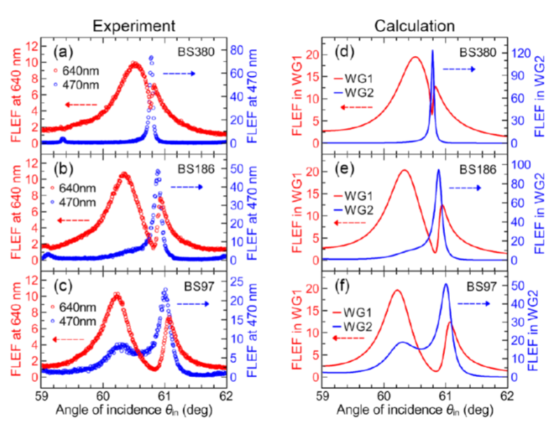
|
Except for a few cases to which sophisticated techniques are applicable, it is difficult to observe experimentally local electric fields or near-fields associated with excitation of electromagnetic modes supported by building blocks of nanostructures. Although elucidating the behavior of the local electric fields or near-fields is very important to develop potential applications of the nanostructures, in many cases, their behaviors have been only speculated from simulations based on the electromagnetic theory. Here, we develop a simple technique that allows us to study experimentally the average behavior of the local electric fields inside two planar waveguide layers interacting with each other in all-dielectric multilayer structures. The study is made possible by doping the two waveguide layers with two different fluorophores. Fluorescence intensities detected at two different wavelengths allow us to study separately the behaviors of the local electric fields inside each waveguide layer. Angle-scan fluorescence excitation spectra are measured for two different series of multilayer samples by exciting the samples in an attenuated total reflection geometry. The line shapes observed are in good agreement with theoretical ones calculated based on the electromagnetic theory, confirming that the experimental fluorescence excitation spectra reflect well the average behaviors of the local electric fields. Applying the developed technique, we investigate systematically the changes in the local electric fields inside the waveguide layers caused by the change in the strength of coupling between the two waveguide modes. In one series of the samples, a gradual transition in the behavior of the local electric fields, from a Fano-resonant behavior to a double-peak behavior, is demonstrated with increasing the coupling strength. In another series of the samples, the coupling strength is widely changed and the formation of the coupled modes in a strong coupling regime is clearly observed. The observed changes in the local electric fields can be reproduced very well by simple analytical calculations based on a coupled oscillator model. The model is helpful to gain physical insights into the coupling of the waveguide modes, which cannot be obtained by the electromagnetic calculations. |
| 319. Robert Turansky, Jan Brndiar, Anton Pershin, Adam Gali, Hiroshi Sugimoto, Minoru Fujii and Ivan ?tich, "Structure and properties of heavily B and P co-doped amorphous silicon quantum dots", The Journal of Physical Chemistry C, Vol. 125, Issue 42, pp.23267-23274 (2021). (Published Online: 15 October 2021) | |
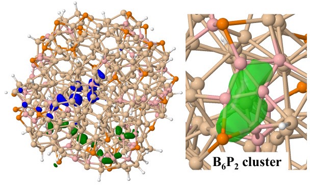
|
Colloidal silicon quantum dots feature a number of outstanding properties, such as size and termination controlled band gap and photoluminescence, which, in combination with nontoxicity, make them suitable for biomedical applications. Because of the presence of structural disorder and experimental limitations, the atomic structure, especially of the small sub 2.5 nm dots, is not well known. We have developed computational techniques that allow us to model the atomic structures of the small dots and have applied them to heavily B and P codoped Si quantum dots and studied their structural, electronic, and vibrational properties. The study confirms that the structures of the smallest dots are fully amorphous with the onset of formation of a quasi-crystalline core in the larger ones. The models give insights into the dopant distribution in the dot. We find that the core morphology depends strongly on the chemical composition of the dot. Study of the electronic and vibrational properties gives insights into their localization properties and allows validation of the generated models by comparison with experiments. The degree of agreement of the properties of our simulated dots with those from experiments suggests that the fine details in preparation protocols may not critically affect their structure and properties. |
| 318. Hiroshi Sugimoto, Hiroaki Hasebe, Taniyuki Furuyama and Minoru Fujii, "Direct excitation of triplet state of molecule by enhanced magnetic field of dielectric metasurfaces", Small, Vol. 17, Issue 47, pp.2104458 (2021). (Published Online: 13 October 2021) | |
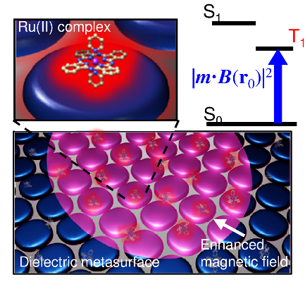
|
Efficient excitation of a triplet (T1) state of a molecule has far-reaching effects on photochemical reaction and energy conversion systems. Because optical transition from a ground singlet (S0) to a T1 state is spin-forbidden, a T1 state is generated via intersystem crossing (ISC) from an excited singlet (S1) state. Although the excitation efficiency of a T1 state can be increased by enhancing ISC utilizing a heavy atom effect, energy loss during ICS (S1→T1 relaxation) is inevitable. Here, we propose a general approach to directly excite a T1 state from a ground S0 state via magnetic dipole transition, which is boosted by enhanced magnetic field induced by a dielectric metasurface. As a dielectric metasurface, we propose a hexagonal array of silicon (Si) nanodisks; the nanodisk array induces strongly enhanced magnetic field on the surface due to the toroidal dipole (TD) resonance. We perform a proof-of-concept experiment using ruthenium (Ru) complexes placed on a metasurface and demonstrate that the phosphorescence is 35-fold enhanced on a metasurface when the TD resonance is tuned to the wavelength of the direct S0→T1 transition. Our results indicate that photon energy necessary to excite the T1 state can be reduced by more than 400 meV compared to the process involving the ISC. By combining optical measurements with numerical simulations, we quantitatively discuss the mechanism of the phosphorescence enhancement. |
| 317. Tatsuki Hinamoto, Minoru Fujii and Takumi Sannomiya, "Optical spin sorting chain", Optics Express, Vol. 29, Issue 22, pp. 34951-34961 (2021). (Published Online: 11 October 2021) | |
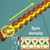
|
Transverse spin angular momentum of light is a key concept in recent nanophotonics to realize unidirectional light transport in waveguides by spin-momentum locking. Herein we theoretically propose subwavelength nanoparticle chain waveguides that efficiently sort optical spins with engineerable spin density distributions. By arranging high-refractive-index nanospheres or nanodisks of different sizes in a zigzag manner, directional optical spin propagation is realized. The origin of efficient spin transport is revealed by analyzing the dispersion relation and spin angular momentum density distributions, being attributed to guided modes that possess transverse spin angular momenta. In contrast to conventional waveguides, the proposed asymmetric waveguide can spatially separate up- and down-spins and locate one parity inside and the other outside the structure. Moreover, robustness against bending the waveguide and its application as an optical spin sorter are presented. Compared to previous reports on spatial engineering of local spins in photonic crystal waveguides, we achieved miniaturization of the entire footprint down to the subwavelength scale. |
| 316. Artyom Assadillayev, Tatsuki Hinamoto, Minoru Fujii, Hiroshi Sugimoto and Soren Raza, "Thermal near-field tuning of silicon Mie nanoparticles", Nanophotonics, Vol. 10, Issue 16, pp.4161-4169 (2021). (Published Online: 1 October 2021) | |
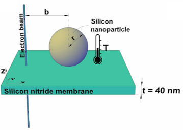
|
Tunable high-refractive-index nanostructures are highly desired for realizing photonic devices with a compact footprint. By harnessing the large thermo-optic effect in silicon, we show reversible and wide thermal tuning of both the far- and near-fields of Mie resonances in isolated silicon nanospheres in the visible range. We perform in situ heating in a transmission electron microscope and electron energy-loss spectroscopy to show that the Mie resonances exhibit large spectral shifts upon heating. We leverage the spectral shifts to demonstrate near-field tuning between different Mie resonances. By combining electron energy-loss spectroscopy with energy-dispersive X-ray analysis, we show a reversible and stable operation of single silicon nanospheres up to a temperature of 1073 K. Our results demonstrate that thermal actuation offers dynamic near-field tuning of Mie resonances, which may open up applications in tunable nonlinear optics, Raman scattering, and light emission. |
| 315. Minoru Fujii, Hiroshi Sugimoto and Shinya Kano, "Colloidal solution of boron and phosphorus codoped silicon quantum dots -from material development to applications", Japanese Journal of Applied Physics, Progress Review, Vol. 61, pp.SA0807 (2021). (Published Online: 10 August 2021) | |
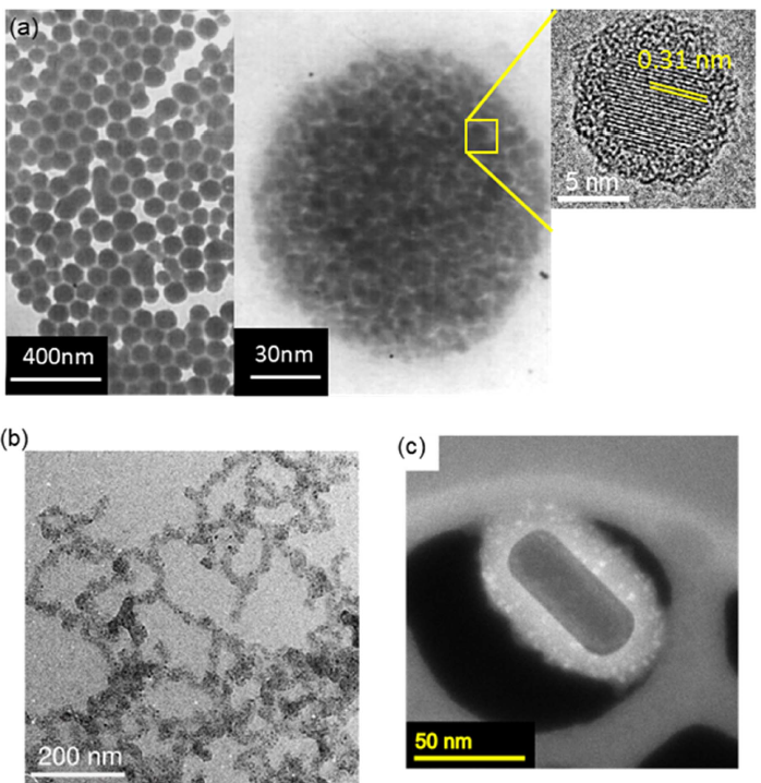
|
A core/shell silicon (Si) quantum dot (QD) composed of a crystalline Si core and an amorphous shell, in which boron (B) and phosphorus (P) are very heavily doped, is developed. Because of the amorphous shell, the B and P codoped Si QDs exhibit significantly different physical and chemical properties from undoped ones. The codoped Si QDs are dispersible in polar solvents such as water and alcohol without organic ligands and exhibit stable luminescence in water. Because of the superior properties, the codoped Si QDs have applications in different fields including photonics, biophotonics, photochemistry and electronics. In this article, we discuss the structure and optical and electrical properties of the codoped core/shell Si QDs and show the application potentials in different fields. |
| 314. Hiroshi Sugimoto and Minoru Fujii, "Colloidal Mie Resonant Silicon Nanoparticles", Nanotechnology, Topical Review, Vol. 32, Number 45, pp.452001 (2021). (Published Online: 3 August 2021) | |
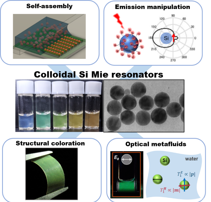
|
Nano- and microstructures of silicon (Si) exhibit electric and magnetic Mie resonances in the optical regime, providing a novel platform for controlling light at the nanoscale and enhancing light?matter interactions. In this Review, we present recent development of colloidal Si nanoparticles (NPs) that have wide range of applications in nanophotonics. Following brief summary of synthesis methods of amorphous and crystalline Si particles with high sphericity, optical responses of single Si particles placed on a substrate are overviewed. Then, the capability as a nanoantenna to control light-matter interactions is discussed in different systems. Finally, collective optical responses of Si NPs in solution are presented and the application potentials are discussed. |
| 313. Miho Takada, Kosuke Inoue, Hiroshi Sugimoto and Minoru Fujii, "Solution-processed silicon quantum dot photocathode for hydrogen evolution", Nanotechnology, Vol. , Issue , pp. (2021). (Published Online: 11 June 2021) | |
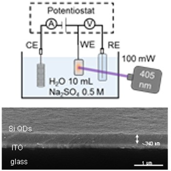
|
The photoelectrochemical response of a photocathode made from a colloidal solution of boron (B) and phosphorus (P) codoped silicon (Si) quantum dots (QDs) 2 to 11 nm in diameters is studied. Since codoped Si QDs are dispersible in alcohol and water due to the hydrophilic surface, a photoelectrode with smooth surface is produced by drop-coating the QD solution on an indium tin oxide (ITO) substrate. The codoping provides high oxidation resistance to Si QDs and makes the electrode operate as a photocathode. The photoelectrochemical response of a Si QD photoelectrode depends strongly on the size of QDs; there is a transition from anodic to cathodic photocurrent around 4 nm in diameter. Below the size, anodic photocurrent due to self-oxidation of Si QDs is observed, while above the size, cathodic photocurrent due to electron transfer across the interface is observed. The cathodic photocurrent increases with increasing the size, and in some samples, it is observed for more than 3000 sec under intermittent light irradiation. |
| 312. Artyom Assadillayev, Tatsuki Hinamoto, Minoru Fujii, Hiroshi Sugimoto, MarkL. Brongersma,and Soren Raza, "Plasmon launching and scattering by silicon nanoparticles", ACS Photonics, Vol. 8, Issue 6, pp.1582-1591 (2021). (Published Online: 19 May 2021) | |
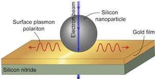
|
Resonant optical nanomaterials with a high refractive index, such as silicon, have become key elements for controlling free-space light. Here, we show that silicon nanoparticles can manipulate highly confined guided waves in the form of surface plasmon polaritons (SPPs) on a subwavelength scale. Using electron energy-loss spectroscopy in a transmission electron microscope, we demonstrate that SPPs in ultrathin metal films can be efficiently launched due to the strong coupling between the Mie resonances of the nanoparticle and the SPP modes. We find that the SPP excitation wavelength can be tuned across the entire near-infrared by varying the particle size. For insight into the coupling mechanism, we also measure the electron-beam-induced response of the Mie resonances in isolated silicon nanostructures in a broad size range. Finally, we show that the silicon nanoparticles act as scatterers of the SPPs supported by the film. Our results may pave the way for using high-refractive-index dielectric nanoantennas as compact elements for manipulating highly confined SPPs. |
| 311. Hiroshi Sugimoto, and Minoru Fujii, "Magnetic Purcell Enhancement by Magnetic Quadrupole Resonance of Dielectric Nanosphere Antenna", ACS Photonics, Vol. 8, Issue 6, pp.1794-1800 (2021). (Published Online: 17 May 2021) | |
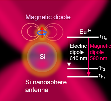
|
Dielectric nanoantennas have been suggested for manipulating the spontaneous emission of a magnetic dipole through the magnetic Purcell effect. However, the experimentally observed enhancement of the magnetic dipole emission has been marginal and much smaller than the theoretical prediction. Here, we develop a composite system, that is, a Si nanosphere decorated with Eu3+ complexes, in which magnetic dipole emission of Eu3+ is efficiently coupled to the magnetic Mie modes of the nanosphere. By means of single particle spectroscopy, we systematically investigate the light scattering and photoluminescence spectra of the coupled system with diameters of Si nanospheres from 130 to 245 nm. We demonstrate that, by tuning the magnetic quadrupole Mie resonance to the 5D0?7F1 magnetic dipole transition of Eu3+, the branching ratio between the magnetic and electric dipole transitions is enhanced up to 7×. We also show the magnetic Purcell enhancement in an ensemble of Si nanospheres with size distribution. |
| 310. Tatsuki Hinamoto, and Minoru Fujii, "MENP: an open-source MATLAB implementation of multipole expansion for nanophotonics ", OSA Continuum, Vol. 4, Issue 5, pp. 1640-1648 (2021). (Published Online: 11 May 2021) | |
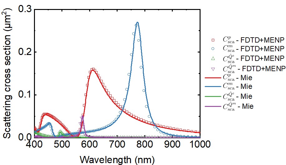
|
In modern nanophotonics, multipolar interference plays an indispensable role to realize novel optical devices represented by metasurfaces with unprecedented functionalities. Not only to engineer sub-wavelength structures that constitute such devices but also to realize and interpret unnatural phenomena in nanophotonics, a program that efficiently carries out multipole expansion is highly demanded. MENP is a MATLAB program for computation of multipole contributions to light scattering from current density distributions induced in nanophotonic resonators. The main purpose of MENP is to carry out post-processing of a rigid multipole expansion for full-field simulations that in principle provide the information of all near- and far-field interactions (e.g., as a total scattering cross section). MENP decomposes total scattering cross sections into partial ones due to electric and magnetic dipolar and quadrupolar terms based on recently developed exact multipole expansion formulas. We validate the program by comparing results for ideal and realistic nanospheres with those obtained with the Mie theory. We also demonstrate the potential of MENP for analysis of anapole states by calculating the multipole expansion under the long-wavelength approximation, which enables us to introduce toroidal dipole moments. |
| 309. Takuma Okazaki, Hiroshi Sugimoto, Tatsuki Hinamoto, and Minoru Fujii, "Color Toning of Mie Resonant Silicon Nanoparticle Color Inks", ACS Applied Materials & Interfaces, Vol. 13, Issue 11, pp. 13613?13619 (2021). (Published Online: 10 March 2021) | |
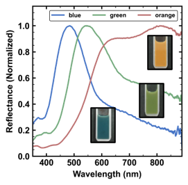
|
An ink of silicon nanoparticles (Si NPs) having the lowest-order Mie resonance in the visible range can generate noniridescent and nonfading structure colors in a wide area by a painting process. However, strong wavelength dependence of the radiation pattern and the extinction coefficient makes the multiple reflection behavior very complicated, and thus a reliable tool is necessary to predict the hue, saturation and brightness of the reflection color. In this work, a Monte Carlo simulation to predict the reflection color of Si NP inks is first developed. The simulation takes into account scattering and absorption cross-sections, a radiation pattern of an individual NP, and multiple scattering in NP dispersion. The simulation shows that reflection color of a Si NP ink depends strongly on the concentration because of the wavelength dependence of the multiple scattering behavior. To extend the controllable range of the hue, saturation and brightness of Si NP inks, a mixture ink with light-absorbing carbon black (CB) NPs is developed. It is experimentally demonstrated that the combination of Kerker-type back scattering of a Si NP and a broad absorption by a CB NP allows us to control the hue, saturation and brightness in a wide range and to realize vivid reflection colors under room light. |
| 308. Ond?ej Pavelka, Sergey A. Dyakov, Jozef Vesely, Anna Fucikova, Hiroshi Sugimoto, Minoru Fujii and Jan Valenta, "Optimizing plasmon enhanced luminescence in silicon nanocrystals by gold nanorods", Nanoscale, Vol. 13, Issue 9, pp. 5045-5057 (2021). (Published Online: 24 February 2021) | |
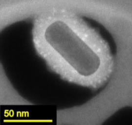
|
The great application potential of photoluminescent silicon nanocrystals, especially in biomedicine, is significantly reduced due to their limited radiative rate. One of the possible ways to overcome this limitation is enhancing the luminescence by localized plasmons of metallic nanostructures. We report an optimized fabrication of gold nanorod ? silicon nanocrystal core-shell nanoparticles with silica shell as a tunable spacer. The unprecedented structural quality and homogeneity of our hybrid nanoparticles allows for detailed analysis of their luminescence. A strong correlation between dark field scattering and luminescence spectra is shown on a single particle level, indicating a dominant role of the longitudinal plasmonic band in luminescence enhancement. The spacer thickness dependence of photoluminescence intensity enhancement is investigated using a combination of experimental measurements and numerical simulations. An optimal separation distance of 5 nm is found, yielding a 7.2x enhancement of the luminescence intensity. This result is mainly attributed to an increased quantum yield resulting from Purcell enhanced radiative rate in the nanocrystals. The ease of fabrication, low cost, long-term stability and great emission properties of the hybrid nanoparticles make them a great candidate for bio-imaging or even targeted cancer treatment. |
| 307. Tatsuki Hinamoto, Mikihiko Hamada, Hiroshi Sugimoto, and Minoru Fujii, "Angle-, Polarization-, and Wavelength-Resolved Light Scattering of Single Mie Resonators Using Fourier-Plane Spectroscopy", Advanced Optical Materials, Vol. 9, Issue 8, pp. 202002192 (2020). (Published Online: 15 February 2021) | |
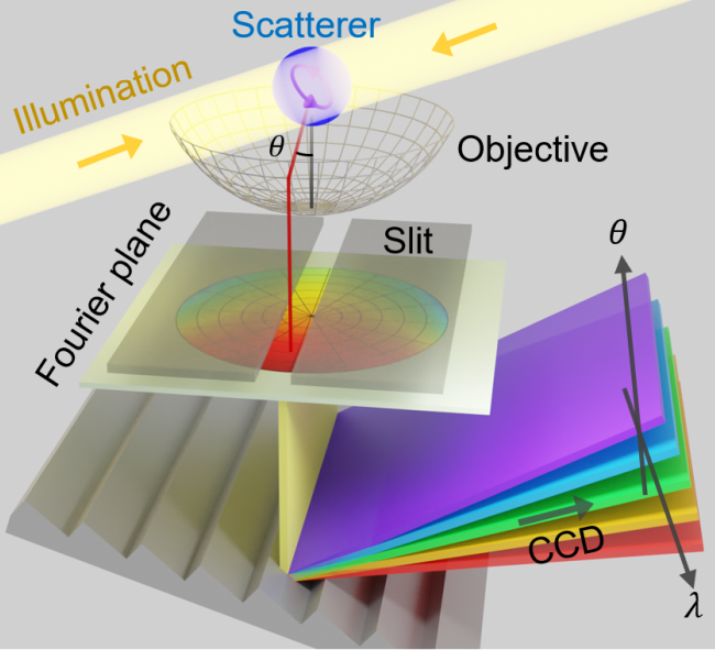
|
Interference between multipole modes of Mie resonance provides the possibility to tailor a radiation pattern of a sub-wavelength optical resonator. Unidirectional scattering arising from constructive and destructive interferences between electric and magnetic dipolar modes in a nanoantenna allows us to design a variety of metasurfaces. However, experimental determination of radiation patterns of an individual nanoobject and the decomposition into multipoles have not been performed under plane wave illumination due to the inability of angular analysis in a conventional optical microscope. To this end, we develop an angle-, polarization-, and wavelengthresolved microscopy setup to measure radiation patterns of an individual nanoobject. We employ a single spherical silicon nanosphere as an ideal Mie resonator and measure the angle- and polarization-resolved scattering in the angular range from 30 to 150° against the incident angle. We show that Mie scattering from the electric and magnetic dipoles of a single silicon nanosphere are selectively measured in the setup. |
| 306. Wanyin Ge, Jindou Shi, Meimei Xu, Yuanting Wu, Hiroshi Sugimoto and Minoru Fujii, "Dual modulating luminescence in all-inorganic perovskite CsPbBr3 quantum dots", Optical Materials, Vol. 113, pp. 110822 (2020). (Published Online: 24 December 2020) | |
|
All-inorganic perovskite quantum dots (AIP QDs) have triggered extensive interest due to their unique optical properties in very recent years. The downconversion (DC) and upconversion (UC) luminescence corresponding to Stokes and anti-Stokes effect are two reverse luminescence phenomena. However, it is seldom to realize these two-reverse luminescence effects in individual QDs simultaneously. Therefore, it is highly desirable to develop comprehensive optical characteristics in order to achieve the multifunction in AIP QDs. Here, colloidal CsPbBr3 perovskite QDs were successfully synthesized by a convenient solution approach. The as-prepared colloidal CsPbBr3 QDs possess highly crystallinity. The DC and UC luminescence properties were studied under ultraviolet (UV) light and infrared (IR) lasers. We have demonstrated that CsPbBr3 QDs exhibited both strong green emission from DC and UC characteristic. In addition, a light-emitting diode device was demonstrated with our CsPbBr3 QDs, showing high-purity green feature. This work reveals the photoluminescence of AIP CsPbBr3 QDs excited by different excitation sources, promoting their multi-functional applications for downconversion and upconversion luminescence. |
| 305. Hiroshi Sugimoto and Minoru Fujii, "Colloidal Mie Resonators for All-Dielectric Meta-Optics", Advanced Photonics Research, Vol. 2, Issue 4, pp. 2000111 (2021). (Published Online: 24 December 2020) | |
|
High refractive index dielectric nanostructures exhibiting electric and magnetic Mie resonances offer a powerful platform for realizing unprecedented control of electromagnetic waves at the nanoscale and enhanced light?matter interactions. Dielectric metasurfaces with a variety of functionalities are realized thanks to recent developments of nanofabrication technologies. In addition, colloidal dispersions of high refractive index dielectric nanoparticles have emerged as a special form of metamaterials that leads to a wider range of applications in photonics. This review focuses on recent developments of colloidal Mie resonators made of moderate (2.5-3.5) to high (>3.5) refractive index dielectrics operating in the visible to near infrared range. Starting from brief summary of fundamental properties of spherical dielectric nanoparticles, fabrication methods of colloidal Mie resonators composed of different materials and optical functionalities such as the enhanced light-matter interactions, the chirality and the structural color generation are overviewed. |
| 304. Asuka Inoue, Hiroshi Sugimoto, Yozo Sugimoto, Kensuke Akamatsu, Marie Hubalek Kalbacova, Chiaki Ogino and Minoru Fujii, "Stable near-infrared photoluminescence from silicon quantum dot?bovineserum albumin composites", MRS Communications, Vol.10, Issue 4, pp.680-686 (2020). (Published Online: 11 November 2020) | |
|
The interaction between negatively charged all-inorganic silicon quantum dots (Si QDs) and bovine serum albumin (BSA) is studied. It is shown that a small difference in the size of Si QDs affects the structure of Si QD?BSA composites significantly. When the diameter of Si QDs is 4 nm, a heterodimer (~20 nm) composed of one Si QD and one BSA molecule is a preferable and stable structure. On the other hand, when the diameter is 7 nm, the size of the composites increases to ~50 nm. The Si QD?BSA composites exhibit stable photoluminescence in the near-infrared range in phosphate-buffered saline. |
| 303. Tatsuki Hinamoto, Shinnosuke Hotta, Hiroshi Sugimoto, and Minoru Fujii, "Colloidal Solutions of Silicon Nanospheres toward All-Dielectric Optical Metafluids", Nano Letters, Vol. 20, Issue 10, pp.7737-7743 (2020). (Published Online: 28 September 2020) | |
|
A colloidal solution of nanophotonic structures exhibiting optical magnetism is dubbed a liquid-phase metamaterial or an optical metafluid. Over the decades, plasmonic nanoclusters have been explored as constituents of a metafluid. However, optical magnetism of plasmonic nanoclusters is usually much weaker than the electric responses; the highest reported intensity ratio of the magnetic-to-electric responses so far is 0.28. Here, we propose an all-dielectric metafluid composed of crystalline silicon nanospheres. First, we address the advantages of silicon as a constituent material of a metafluid among major dielectrics. Next, we experimentally demonstrate for the first time that a silicon nanosphere metafluid exhibits strong electric and magnetic dipolar Mie responses across the visible to near-infrared spectral range. The intensity ratio of the magnetic-to-electric responses reaches unity. Finally, we discuss the perspective to achieve unnaturally high (> 3), low, and even near-zero (< 1) refractive index in the metafluid. |
| 302. Hiroaki Hasebe, Hiroshi Sugimoto, Tatsuki Hinamoto, Minoru Fujii, "Coupled Toroidal Dipole Modes in Silicon Nanodisk Metasurface: Polarization Independent Narrow Band Absorption and Directional Emission", Advanced Optical Materials, Vol. 20, Issue 22 pp.2001148 (2020). (Published Online: 24 June 2020) | |
 |
Besides the fundamental Mie resonance modes of high‐index dielectric nanostructures, an extended multipole family, i.e., toroidal multipoles, provide great opportunities for engineering a new class of nanophotonic devices. Here, it is demonstrated theoretically and experimentally that a hexagonal array of circular silicon (Si) nanodisks (NDs) supports intra‐ and inter‐ND toroidal dipole (TD) modes. The key concept is the alignment of Si NDs near the anapole state condition for constructive interaction of the TD modes between neighboring NDs. Numerical simulation reveals that strong field confinement by the coupled TD modes enhances the absorption 120‐fold at the resonance wavelength compared to that of a flat Si film with the same thickness. In this study, macroscopic scale hexagonal Si ND arrays are fabricated using a colloidal lithography, and spectrally selective absorption enhancement due to the TD modes is demonstrated. Furthermore, it is demonstrated that a dipolar emitter can also excite TD modes, which modify the spectral shape and the directionality of the emission. |
| 301. Hiroshi Sugimoto, Ryosuke Imaizumi, Tatsuki Hinamoto, Takahiro Kawashima, Minoru Fujii, "Silicon Nanowire on Mirror Nanoantennas -Engineering Hybrid Gap Mode for Light Sources and Sensing Platforms", ACS Applied Nano Materials, Vol. 3, Issue 7, pp. 7223-7230 (2020). (Published Online: 24 June 2020) | |
 |
It has been demonstrated recently that a nanowire (NW) of high refractive index dielectric materials works as a novel nanoantenna owing to the excitation of the Mie-type resonances. Here, we explore the capability of a silicon (Si) NW as an optical nanoantenna by combining it with an external metallic component. We investigate the light scattering property of a single Si NW placed on a gold (Au) mirror via a very thin dielectric spacer and demonstrate strong confinement of electromagnetic fields in the gap owing to the coupling of the resonance modes with a Au mirror. We demonstrate that the resonance wavelength of the hybrid mode can be tuned by the gap length, and the hybrid gap mode strongly modifies the spectral shape of the emission from a quantum dot (QD) monolayer incorporated in the gap. Quantitative analyses of the data in combination with numerical simulations reveal that the enhancement and the polarization control of the QD emission is achieved by the coupling. |
| 300. Byungjun Kang, Kengo Motokura, Minoru Fujii, Dmitry V. Nesterenko, Zouheir Sekkat, and Shinji Hayashi, "Observation of Fano Line Shape in Directional Fluorescence Emission Mediated by Coupled Planar Waveguide Modes and Interpretation Based on Lorentz Reciprocity ", AIP Advances, Vol. 10, Issue 7, pp.075302 (2020). (Published Online: 1 July 2020) | |
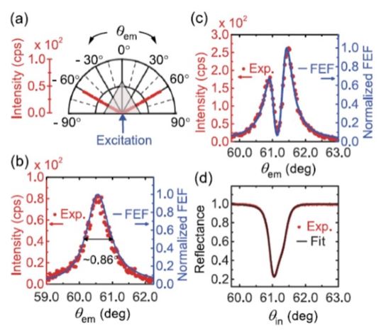 |
Using a reverse attenuated-total-reflection geometry, we measured angle-scan fluorescence emission spectra of all-dielectric multilayer samples containing a waveguide layer doped with fluorescent dye molecules (fluorescent waveguide layer). A sample containing only one fluorescent waveguide layer showed a highly directional emission spectrum with a Lorentzian line shape caused by radiative decay of an excited planar waveguide mode into a travelling wave in a decoupling prism. Addition of another waveguide layer containing absorptive dye molecules was found to greatly modify the spectrum and generate a Fano line shape in the emission spectrum. The observed Lorentzian and Fano emission spectra could be well reproduced by electromagnetic calculations based on the Lorentz reciprocity theorem. Calculated results of electric field distributions indicate that the Fano line shape is generated by suppression of local electric fields inside the fluorescent waveguide layer resulting from coupling between two waveguide modes. |
| 299. Jing Huang, Jingjian Zhou, Tommy Haraldsson, Alden Clemments, Minoru Fujii, Hiroshi Sugimoto, Bo Xu and Ilya Sychugov, "Triplex Glass Laminates with Silicon Quantum Dots for Luminescent Solar Concentrators", Solar RRL, Vol. 7, Issue 9, pp.2000195 (2020). (Published Online: 16 June 2020) | |
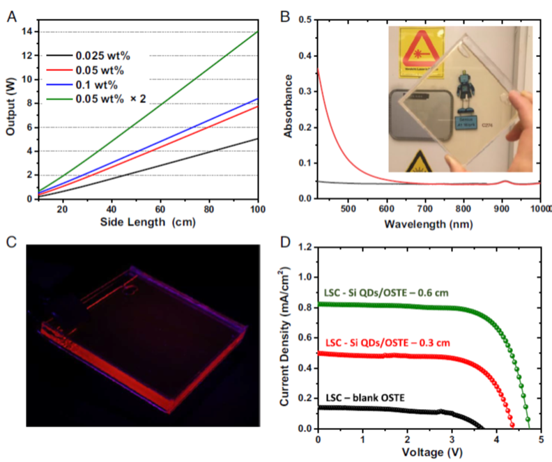 |
Luminescent solar concentrator (LSC) is a promising technology to integrate a semi-transparent photovoltaic (PV) system into modern buildings and vehicles. Silicon quantum dots (QDs) are good candidates as fluorophores in LSCs, due to the absence of overlap between absorption and emission spectra, recorded high photoluminescence quantum yield (PLQY), good stability, non-toxicity and element abundance. In this work, LSCs based on Si QDs/polymer nanocomposites were fabricated in a triplex glass configuration. A special polymer matrix (off-stoichiometric thiol-ene, OSTE) was used, which improves nanocrystal quantum yield and can be directly integrated with glass due to minimal polymerization shrinkage. Here we conducted a comprehensive investigation to improve the performance of LSCs, by exploring effective strategies under the guidance of a theoretical description. Among these strategies, one of the most two effective ones are systematical enhancement of PLQY of the nanocomposite by tuning thiol/allyl ratio in OSTE matrix. The other one is ligand selection and loading optimization for QDs to reduce the total scattering loss in the device. As a preliminary result, the LSC prototype (9 × 9 × 0.3 cm3) fabricated with optimized nanocomposite has an estimated optical efficiency of ~3.4% at a high transmittance of 79% at 500 nm. The efficiency can be further improved by increasing absorption (thickness of the LSC) and the quantum yield of the QDs, while better nanoparticle dispersion can further reduce scattering losses. Proposed here systematic examination of the device losses will facilitate comparison between different material systems and designs for successful LSC implementation. |
| 298. Minoru Fujii, Riku Fujii, Miho Takada, and Hiroshi Sugimoto, "Silicon Quantum Dot Supraparticles for Fluorescence Bioimaging", ACS Applied Nano Materials, Vol. 3, Issue 6, pp.6099-6107 (2020). (Published Online: 18 May 2020) | |
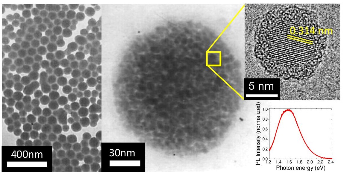 |
We developed a self-limited self-assembly process to produce red-to-near-infrared luminescent supraparticles made from bio-compatible silicon (Si) quantum dots (QDs) for fluorescence bio-imaging. A starting material is a methanol solution of boron (B) and phosphorus (P) codoped all-inorganic Si QDs. The Si QDs have a heavily B and P codoped amorphous shell and the shell induces negative potential on the surface, which prevents agglomeration of QDs in polar solvents. By adding toluene to the methanol solution, controlled agglomeration of Si QDs occurs and spherical supraparticles around 100 nm in diameter with a narrow size distribution are grown. The average diameter of supraparticles was controlled by the growth parameters. We also developed a process to stabilize the supraparticles by coating the surface by polyvinylpyrrolidone (PVP) and then by silica. The photoluminescence spectra of PVP- and silica-coated Si QDs supraparticles were very similar to those of Si QDs dispersed in solution. |
| 297. Hiroshi Sugimoto, Takuma Okazaki, and Minoru Fujii, "Mie Resonator Color Inks of Monodispersed and Perfectly Spherical Crystalline Silicon Nanoparticles", Advanced Optical Materials, Vol. 8, Issue 12 pp. 2000033 (2020). (Published Online: 5 May 2020) | |
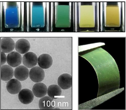 |
A crystalline silicon (Si) nanoparticle (NP) of 100?200 nm in diameter exhibits a highly saturated color owing to Mie resonance, and can be a component to realize angle-insensitive structural color covering the entire visible range. However, to date, coloring a substrate by Si nanostructures has only been achieved in a very small area by using electron beam lithography and dry etching processes. In this work, we develop a Si NP color ink capable of coloring a flexible substrate by a painting process. The sphericity of Si NPs is very high; the circularity factor obtained from a transmission electron microscope image reaches 0.97. The average diameter of Si nanospheres is controlled from 95 to 200 nm, and the polydispersity defined by the standard deviation divided by the average diameter is as small as 6%. Because of the high sphericity, high crystallinity, high size purity, and perfect dispersion in solution, the Si nanosphere solutions exhibit vivid colors recognizable by naked eye in a range of blue to orange. The Si nanosphere color inks combined with a polymer binder are capable of coloring flexible substrates by a painting process. |
| 296. Minoru Fujii, Akiko Minami, and Hiroshi Sugimoto, "Precise size separation of water-soluble red-to-near-infrared-luminescent silicon quantum dots by gel electrophoresis", Nanoscale, Vol. 12, Issue 16, pp. 9266-9271 (2020). (Published Online: 10 April 2020) | |
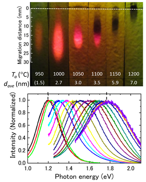 |
A gel electrophoresis, which is a standard method for separation and analysis of macromolecules such as DNA, RNA and proteins, is applied for the first time to silicon (Si) quantum dots (QDs) for the size separation. In the Si QDs studied, boron (B) and phosphorus (P) are simultaneously doped. The codoping induces negative potential on the surface of a Si QD and makes it dispersible in water. It is shown that a gel electrophoresis can separate codoped Si QDs by size with very high resolution. The capability of gel electrophoresis to immobilize size-separated QDs in a solid matrix makes detailed analyses of size-purified Si QDs possible. Photoluminescence studies of dried gels demonstrate that a broad PL spectrum of a Si QDs solution can be separated into more than 15 spectra of size-purified Si QDs. |
| 295. Keita Nomoto, Hiroshi Sugimoto, Anna V. Ceguerra, Minoru Fujii, and Simon Ringer, "3D microstructure analysis of silicon-boron phosphide mixed nanocrystals", Nanoscale, Vol. 13, Issue 12, pp. 7256-7262 (2020). (Published Online: 12 March 2020) | |
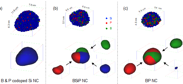 |
The microstructure of boron (B) and phosphorus (P) codoped silicon (Si) nanocrystals (NCs), cubic boron phosphide (BP) NCs and their mixed NCs (BxSiyPz NCs) has been studied using atom probe tomography (APT), transmission electromicroscopy (TEM), and Raman scattering spectroscopy. The BxSiyPz NCs inherit superior properties of B and P codoped Si NCs such as high dispersibility in aqueous media and near infared (NIR) luminescence and those of cubic BP NCs such as the high chemical stability. The microanalyses revealed that BxSiyPz NCs are composed of a crystalline core and an amorphous shell. The core possesses a lattice constant between that of Si (diamond-cubic) and BP (cubic). The amorphous shell is comprised of B, Si and P, though the composition is not uniform and there are local B-rich, Si-rich and P-rich domains connected contiguously. The amorphous shell is proposed to be responsible for the superior chemical properties such as the high dispersibility in polar solvents and high resistance to acids, and the crystalline core is responsible for the stable NIR luminescence. |
| 294. Hiroshi Sugimoto, Hao Zhou, Miho Takada, Junichiro Fushimi, and Minoru Fujii, "Visible-Light Driven Photocatalytic Hydrogen Generation by Water-Soluble All-Inorganic Core-Shell Silicon Quantum Dots", Journal of Materials Chemistry A, Vol. 8, Issue 31, pp. 15789-15794 (2020). (Published Online: 25 February 2020). Invited paper for Journal of Materials Chemistry A "Emerging Investigators 2020". | |
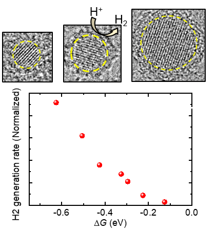 |
The photocatalytic hydrogen (H2) generation by boron (B) and phosphorus (P) codoped silicon quantum dots (Si QDs) with diameters in the quantum confinement regime is investigated. The codoped Si QDs have an amorphous shell made from B, Si and P. The shell induces negative potential on the surface and makes codoped Si QDs dispersible in water. The hydrophilic shell offers enhanced stability and efficiency in the photocatalytic H2 generation and provides the opportunity to study the size dependence of the H2 generation rate. A drastic increase of the H2 generation rate with decreasing the QD size is observed. Analyses based on the Marcus theory reveal that the upper shift of the lowest unoccupied molecular orbital level of Si QDs by the quantum confinement effect is responsible for the enhanced photocatalytic activity. |
| 293. Kengo Motokura, Byungjun Kang, Minoru Fujii, Dmitry V. Nesterenko, Zouheir Sekkat, and Shinji Hayashi, "Wide-range line shape control of Fano-like resonances in all-dielectric multilayer structures based on enhanced light absorption in photochromic waveguide layers", Journal of Applied Physics, Vol. 127, Issue 7, pp. 073103 (2020). (Published Online: 18 February 2020) | |
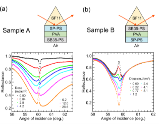 |
We have succeeded in controlling the line shape of Fano-like resonances in all-dielectric multilayer structures in a wide range by UV light irradiation. Multilayer structures consisting of a waveguide layer supporting a half-leaky guided mode, a spacer layer, and another waveguide layer supporting a planar waveguide mode are known to exhibit Fano-like line shapes in attenuated total reflection spectra due to coupling between the half-leaky guided mode and the planar waveguide mode. Using a photochromic layer, i.e., a layer doped with spiropyran molecules, as one of the waveguide layers, we controlled the amount of light absorption in the waveguide layer by varying the UV irradiation dose. We demonstrated that the line shape changes dramatically depending on the UV dose, from the electromagnetically induced transparency-like to electromagnetically induced absorption-like line shape (or vice versa) passing through the Fano-like line shape. We also demonstrated that the photochromic response induced by UV irradiation in the Fano-resonant multilayer structure is enhanced by a factor of ?100 relative to that in a single photochromic layer. Our analyses based on electromagnetic calculations suggest that the dramatic line shape change and the enhanced photochromic response are the consequences of enhanced local electric fields inside the photochromic waveguide layer combined with the photoinduced increase in the imaginary part of the dielectric constant. |
| 292. John A. Parker, Hiroshi Sugimoto, Brighton Coe, Daniel Eggena, Minoru Fujii, Norbert F. Scherer, Stephen K. Gray, and Uttam Manna, "Excitation of nonradiating anapoles in dielectric nanospheres", Physical Review Letters, Vol. 124, Issue 9, pp. 097402 (2020). (Published 6 March 2020) | |
 |
Although the study of non-radiating anapoles has long been part of fundamental physics, the dynamic anapole at optical frequencies was only recently experimentally demonstrated in a specialized silicon nanodisk structure. We report excitation of the electrodynamic anapole mode in isotropic silicon nanospheres using radially polarized beam illumination. The superposition of equal and out-of-phase amplitudes of the Cartesian electric and toroidal dipoles produces by a pronounced dip in the scattering spectra with the scattering intensity almost reaching zero - a signature of anapole excitation. The total scattering intensity associated with the anapole excitation is found to be more than 25 times weaker for illumination with radially vs. linearly polarized beams. Our approach provides a simple, straightforward alternative path to realize electrodynamic anapole mode at the optical frequencies. |
| 291. Ruma Das, Hiroshi Sugimoto, Minoru Fujii and Pravat K. Giri, "Quantitative Understanding of Charge Transfer Mediated Fe3+ Sensing and Fast Photoresponse by N-doped Graphene Quantum Dots Decorated on Plasmonic Au Nanoparticles", ACS Applied Materials & Interfaces, Vol. 12, Issue 4, pp. 4755-4768 (2020). (January 8 November 2020) | |
 |
The formation of heterostructure with plasmonic nanoparticles drastically alter the optoelectronic properties of graphene quantum dots (GQDs), resulting in exceptional properties. In the present work, we prepare nitrogen-doped GQDs decorated on gold nanoparticle (Au@N-GQDs) by a one-step green reduction method and study its extraordinary fluorescence and photoresponse characteristics. The as-prepared Au@N-GQDs show more than one order of magnitude enhancement in the fluorescence intensity as compared to the bare N-GQDs, which is attributed to hot electron generation and improved absorption in N-GQDs by local field enhancement and the modification of the edge functional groups. Due to the selective coordination to Fe3+ ions, the Au@N-GQDs exhibit extraordinary quenching of fluorescence, with ultrahigh sensitivity for the detection of Fe3+ (<1 nM). A new model for the charge transfer dynamics is developed involving the Langmuir’s law of adsorption to explain the unusual quenching, which strongly deviates from the known models of static/ dynamic quenching. The proposed sensor is successfully implemented for the ultrasensitive detection of Fe3+ ions in human serum and Brahmaputra river water samples, representing its high potential applications in clinical as well as environmental diagnosis. Additionally, due to its high absorption in the UV-Vis-NIR region and high charge density with long life excitons, the Au@N-GQDs is utilized as a photodetector with ~104 times faster response than that of bare N-GQDs. The Au@N-GQDs based photodetector possesses a high responsivity of ~1.36 A/W and a remarkably high external quantum efficiency of ~292.2 %, which is much superior to the GQDs based photodetectors reported till date. The underlying mechanism of ultrafast photoresponse is ascribed to the transfer of hot electrons along with the tunneling of the electrons from Au NPs to N-GQDs as well as the defect reduction of N-GQDs by the incorporation of Au NPs. Without the use of any charge transporting layer, the outstanding performance of N-GQDs based plasmonic photodetector opens up unique opportunities for future high-speed optoelectronic devices. |
| 290. Uttam Manna, Hiroshi Sugimoto, Daniel Eggena, Brighton Coe, Ren Wang, Mahua Biswas, and Minoru Fujii, "Selective excitation and enhancement of multipolar resonances in dielectric nanospheres using cylindrical vector beams", Journal of Applied Physics, Vol. 127, Issue 3, pp. 033101 (2020). (Published Online: 2020) | |
|
Resonant excitation and manipulation of complex interactions among two or more resonances in high-index dielectric nanostructures provide great opportunities for engineering novel optical phenomena and applications. However, difficulties often arise when interpreting the observed spectra because of the overlap of the broad resonances contributed by many factors such as particle size, shape, and background index. Therefore, selective excitation of resonances that spectrally overlap with each other provides a gateway towards improved understanding of the complex interactions. Here, we demonstrate selective excitation and enhancement of multipolar resonances of silicon nanospheres using cylindrical vector beams (CVBs) with different diameters of nanospheres and numerical apertures (NAs) of the excitations. By combining single particle spectroscopy and electrodynamic simulations, we show that the radially polarized beam can selectively excite the electric multipoles, whereas the azimuthally polarized beam can selectively excite the magnetic multipoles even though the multipolar resonances are convoluted together due to their spectral overlap. Moreover, focusing the CVBs with high NA can lead to dominant longitudinal polarization of the electric or magnetic field. We show that the enhanced longitudinal polarization with increasing NA of the radially and azimuthally polarized beams can selectively enhance the electric and magnetic multipolar resonances, respectively. Our approach can be used as a spectroscopy tool to enhance and identify multipolar resonances leading to a better understanding of light-matter interactions in other dielectric nanostructures; as well as serve as a first step towards excitation of dark mode and Fano resonances in dielectric oligomers by breaking the symmetry of the nanostructures. |
| 289. Hiroto Yanagawa, Tatsuki Hinamoto, Takashi Kanno, Hiroshi Sugimoto, Masahiko Shioi, and Minoru Fujii, "Gold nanopillar array with sharp surface plasmon resonances and the application in immunoassay", Journal of Applied Physics, Vol. 126, pp. 223104 (2019). (Published Online: 12 December 2019) | |
|
Nano-imprinting followed by metal deposition is a low-cost, high-throughput and highly-reproducible process for the fabrication of large-size plasmonic substrates required for commercial products. However, the plasmonic substrates prepared by the process usually has very broad surface plasmon resonances, which cannot be well-reproduced by numerical simulations. The poor agreement between experiments and calculations has prevented detailed analysis of the field enhancement behavior and the improvement of the performance as plasmonic substrates. In this work, we demonstrate that large-area plasmonic substrates with sharp surface plasmon resonances, that can be well-reproduced by numerical simulations, are produced by sputter-deposition of gold (Au) on a commercially-available nano-imprinted substrate. The good agreement between experiments and simulations allow us to identify the locations and field distributions of the hot spots. Angle dependence of specular reflectance and diffuse reflectance measurements in combination with numerical simulations reveal that a dipole-like bright mode and a higher-order dark mode exist at gaps between Au nanorods. Finally, we demonstrate the application of the developed plasmonic substrates for surface-enhanced fluorescence in sandwich immunoassays for the detection of influenza virus nucleoprotein. We show that the sharp resonance and the capability of precise tuning of the resonance wavelength significantly enhance the luminescence signal. |
| 288. Takeshi Kawauchi, Shinya Kano, and Minoru Fujii, "Electrically stimulated synaptic resistive switch in solution-processed silicon nanocrystal thin film: formation mechanism of oxygen vacancy filament for synaptic function", ACS Applied Electronic Materials. Vol. 1, Issue 12, pp. 2664-2670 (2019). (Published Online: 18 November 2019) | |
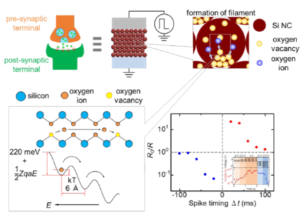 |
We demonstrate an electrically stimulated synaptic resistive switch in a silicon nanocrystal (Si NC) thin film. A forming-free resistive switching occurs on the surface of natively oxidized Si NCs due to filaments of oxygen vacancies. To show a gradual change of the resistance, we investigate a formation mechanism of an oxygen vacancy filament. This gradual change of the resistance with input voltage pulses corresponds to short-term plasticity (STP) and long-term potentiation (LTP) in biological synapses. We simulate spike timing dependent plasticity (STDP) in the resistive switch by voltage pulses. |
| 287. Tatsuki Hinamoto, Tomoki Higashiura, Hiroshi Sugimoto, and Minoru Fujii, "Elongated Metal Nanocap with Two Magnetic Dipole Resonances and Its Application for Upconversion Enhancement", J. Phys. Chem. C, Vol. 123, Issue 42, pp. 25809-25815 (2019). (Published Online: 4 Octorber 2019) | |
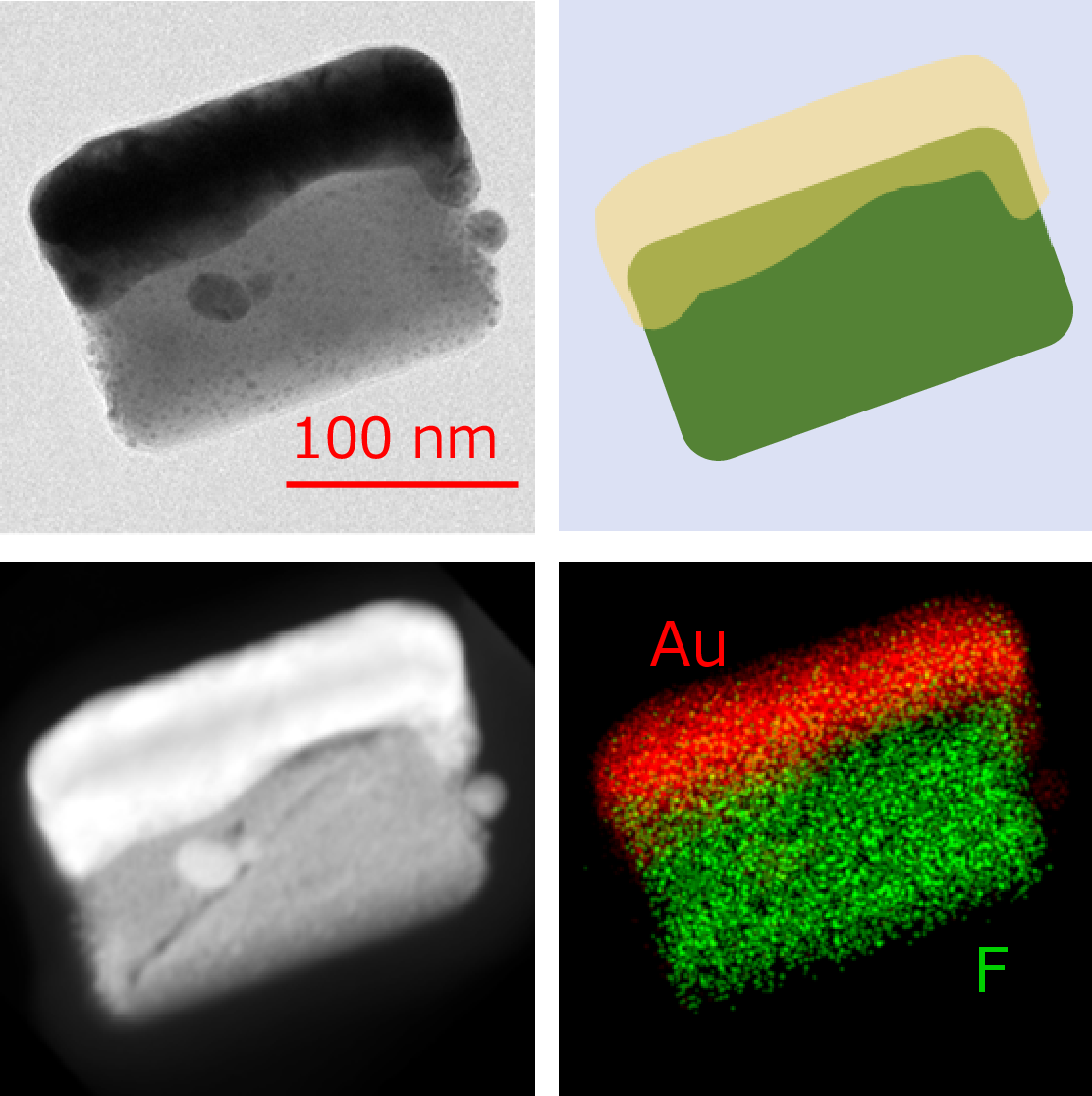 |
A stand-alone plasmonic nanocomposite into which a metal nanostructure and an emitting material are integrated is a promising building block for optoelectronics and biophotonics devices. Here we present the plasmonic property of a nanocomposite composed of a Au elongated nanocap and a β-NaYF4 dielectric nanorod. We show that elongation of a Au nanocap results in splitting of the magnetic dipole resonance, and the resonance wavelengths can be controlled in a wide wavelength range by the aspect ratio. As an application of the elongated nanocap, we demonstrate strong enhancement of the near-infrared to visible upconversion of an Er3+ and Yb3+ doped β-NaYF4 nanorod by tuning the resonance wavelength of a Au nanocap placed on it to the excitation wavelength. |
| 286. Byungjun Kang, Kengo Motokura, Minoru Fujii, Dmitry Nesterenko, Zouheir Sekkat, and Shinji Hayashi, "Fano resonant behaviour of waveguide mode in all-dielectric multilayer structure directly monitored by fluorescence of embedded dye molecules", Journal of Optics, Vol. 21, pp. 105006 (2019). (Published Online: 10 November 2019) | |
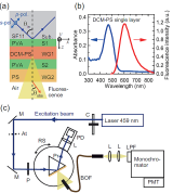 |
A method that allows direct monitoring of Fano resonant behaviours of local electric fields inside a waveguide layer in multilayer structures was developed. All-dielectric multilayer structures consisting of two polystyrene waveguide layers separated by a polyvinyl alcohol spacer layer were prepared. One of the waveguide layers was doped with fluorescent dye molecules. The fluorescence spectra of the sample were measured in a Kretschmann attenuated-total-reflection geometry as a function of the angle of incidence of the excitation light. The angle-scan fluorescence excitation spectra exhibited a sharp Fano line shape superposed on a broad band. Results of electromagnetic calculations of the electric field distribution inside the multilayer structure revealed that the local electric fields inside the dye-doped waveguide layer exhibit Fano resonant behaviours due to the near-field coupling to the waveguide mode supported by another waveguide layer. Using the calculated local electric fields, theoretical fluorescence spectra were calculated based on a point dipole model. The theoretical fluorescence spectra were found to reproduce very well the experimental ones, confirming that the observed Fano line shapes in the fluorescence spectra are the manifestation of the Fano resonant behaviours of the local electric fields inside the dye-doped layer. |
| 285. Hiroshi Sugimoto, Yoichi Ikuno and Minoru Fujii, "Absolute Scattering Cross-Sections of Titanium Nitride Nanoparticles Determined by Single-Particle Spectroscopy: Implications for Plasmonic Nanoantennas", ACS Applied Nano Materials, Vol. 2, Issue 10, pp. 6769-6773 (2019). (Published Online: 11 September 2019) | |
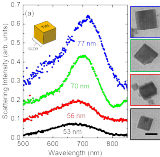 |
Titanium nitride (TiN) nanostructures are promising building blocks for photothermal applications because of the surface plasmon-induced light absorption. However, compared to noble metal nanostructures, detailed analyses of the plasmonic responses of TiN nanostructures have been limited. In this work, by combining transmission electron microscopy (TEM) and single-particle spectroscopy, we determine absolute scattering cross-sections of individual TiN nanocubes (NCs). The key aspect of the developed methodology is placing a TiN NC on an ultrathin SiO2 membrane and performing the precise structural analysis and the scattering spectrum measurement on identical TiN NCs. Furthermore, by employing Au nanospheres as references, we quantitatively compare the scattering spectra with those obtained for TiN NCs and determine the absolute scattering cross-section as a function of NC size. |
| 284. Hiroshi Sugimoto, Balint Somogyi, Toshiyuki Nakamura, Hao Zhou, Yuichi Ichihashi, Satoru Nishiyama, Adam Gali and Minoru Fujii, "Size-Dependent Photocatalytic Activity of Cubic Boron Phosphide Nanocrystals in the Quantum Confinement Regime", The Journal of Physical Chemistry C, Vol. 123, pp.23266-23235 (2019). (Published Online: 21 August 2019) | |
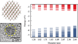 |
Cubic boron phosphide (BP) is an indirect band gap semiconductor with a band gap of 2.0 eV and promising for a highly stable photocatalyst to produce hydrogen from water under visible light irradiation. Here, we performed a comprehensive study on the energy-level structure and photocatalytic activity of BP nanocrystals (NCs) in the quantum confinement regime (<5 nm in diameter). First, we calculated the electronic structure of cubic BP NCs up to 2.8 nm in diameter, hexagonal BP nanoflakes, and cubic/hexagonal BP nanostructures by density functional theory and time-dependent density functional theory. We then synthesized BP NCs with 2?13 nm in diameters and performed detailed structural analyses and optical measurements. The photocatalytic bleaching experiments for dye molecules under visible light irradiation revealed that the bleaching rate depends strongly on the size of BP NCs; the increase in the band gap of BP NCs by the quantum size effects (QSE) enhanced the photocatalytic activity. The band gap increase by the QSE also enhanced the rate of photocatalytic hydrogen evolution |
| 283. Keita Nomoto, Hiroshi Sugimoto, Xiang-Yuan Chi, Anna V. Ceguerra, Minoru Fujii, and Simon P. Ringer,
"Distribution of Boron and Phosphorus and Roles of Co-Dopingin Colloidal Silicon Nanocrystals",
Acta Materialia, Vol. 178, pp.186-193 (2019). (Published Online: 15 August 2019) |
|
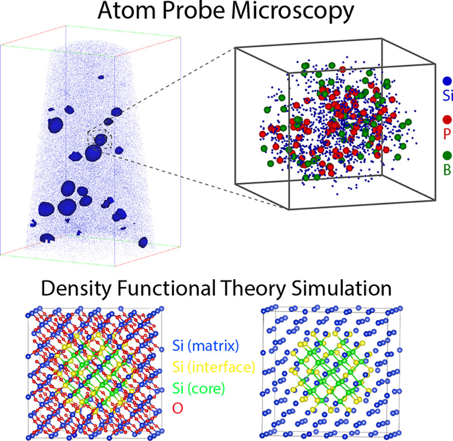 |
Boron (B) and phosphorous (P) co-doped colloidal silicon nanocrystals (Si NCs) have unique size-dependent optical properties, which lead to potential applications in optoelectronic and biomedical applications. However, the microstructure of the B and P co-doped colloidal Si NCs ? in particular, the exact location of the dopant atoms in real space, has not been studied. A lack of understanding of this underlying question limits our ability to better control sample fabrication, as well as our ability to further develop the optical properties. To study the microstructure, a process enabling atom probe tomography (APT) of colloidal Si NCs was developed. A dispersion of colloidal Si NCs in a SiO2 sol-gel solution and a low temperature curing are demonstrated as the key sample preparation steps. Our APT results demonstrate that a B-rich region exists at the surface of the Si NCs, while P atoms are distributed within the Si NCs. First principles density functional theory calculations of a Si NC embedded in SiO2 matrix reveal that P atoms, which always prefer to reside inside a Si NC, significantly influence the distribution of B atoms. Specifically, P atoms lower the B diffusion barrier at Si/SiO2 interface and stabilize B atoms to reside within individual Si NCs. We propose that the B-modified surface changes the chemical properties of the Si NCs by (i) offering chemical resistance to attack by HF and (ii) enabling dispersibility in solution without aggregation. |
| 282. Hiroshi Sugimoto, Tatsuki Hinamoto, and Minoru Fujii, "Forward to Backward Scattering Ratio of Dielectric-Metal Heterodimer Suspended in Almost Free-Space", Advanced Optical Materials, Vol. 7, Issue 20, pp. 1900591 (2019). (Published Online: 07 August 2019) | |
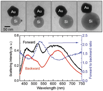 |
A designed nanoantenna exhibiting unidirectional scattering is a promising building block for novel nanophotonic devices. For device applications using nanoantennas, quantitative information on the directional scattering property is indispensable. However, experimental determination of the forward to backward scattering intensity ratio of a nano‐object is not straightforward. Here, a scheme to determine the ratio quantitatively is proposed. A key technology of the scheme is placing a nano‐object on a thin SiO2 membrane. Because of the low refractive index and the small thickness of the membrane, the nano‐object can be treated as being suspended in free‐space. This allows us to use an ideal Mie scatterer such as a spherical silicon (Si) nanocrystal as a reference to calibrate optical setups for the measurements of forward and backward scattering. Using the developed scheme, the directional scattering property of a heterodimer composed of Si and gold nanospheres synthesized by a solution process is investigated. By combining transmission electron microscopy and scattering measurements, systematic studies on the directional scattering property of a heterodimer by changing the size of a Si nanosphere is performed. It is demonstrated that strong Kerker‐type forward scattering is achieved by tuning the resonance wavelength of the magnetic dipole resonance of a Si nanosphere. |
| 281. Hiroto Yanagawa, Asuka Inoue, Hiroshi Sugimoto, Masahiko Shioi, and Minoru Fujii, "Antibody-conjugated near-infrared luminescent silicon quantum dots for biosensing", MRS Communications, Vol. 9, Issue 3, pp. 1079-1086 (2019). (Published Online: 26 July 2019) | |
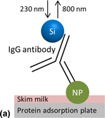 |
A process for bioconjugation of an IgG antibody and silicon quantum dots (Si-QDs) having the luminescence in the near-infrared (NIR) range was developed. For the bioconjugation, the surface of water-soluble all-inorganic Si-QDs was functionalized by using silane-coupling agents. In amino-functionalized Si-QDs, successful conjugation was achieved without strongly affecting the luminescence property. Detailed analyses revealed that Si-QDs are bound covalently to both the light and heavy chains of an IgG antibody. It was also confirmed that the binding property of an IgG antibody with antigen nucleoprotein was not ruined by the process. The successful conjugation of an IgG antibody and NIR luminescent Si-QDs paves the way for designing environmentally friendly bio-sensing and -imaging processes. |
| 280. Kamal Kumar Paul, P. K. Giri, Hiroshi Sugimoto, Minoru Fujii, and Biswajit Choudhury, "Evidence for plasmonic hot electron injection induced superior visible light photocatalysis by g-C3N4 nanosheets decorated with Ag?TiO2(B) and Au?TiO2(B) nanorods", Solar Energy Materials and Solar Cells, Vol. 201, pp. 110053-1-12 (2019). (Published Online: 18 July 2019) | |
 |
Hot electrons produced by the surface plasmon decay can be efficiently utilized to drive photochemical reactions on a semiconductor surface. Considering this aspect of plasmonics, we have evaluated the visible light photocatalytic performance of Ag?TiO2(B)?C3N4 and Au?TiO2(B)?C3N4 heterostructures in the degradation of rhodamine B (RhB) and phenol. The synergetic effect of plasmonic hot electron injection and interfacial charge transfer in the heterostructures lead to 6?9 fold enhancement in the photodecomposition rate of RhB (phenol) over TiO2(B) and C3N4. Time-resolved photoluminescence study shows fast charge transfer through the integrated network of the heterostructure. The photocurrent is measured at 470?nm, 510?nm and 575?nm, near the plasmonic excitations of Ag and Au as well as under white light illumination (400?800?nm). Plasmonic systems show more than 6-fold enhancement in photocurrent over bare TiO2(B) under illumination near monochromatic plasmonic excitation. The overall photocurrent resulting from white light illumination is 2-fold stronger than that under plasmonic excitation. The increase is due to the contribution from Ti3+ excitation, hot electron injection, and charge transfer from TiO2(B) to C3N4. We propose that Ti3+ states in TiO2(B) provide channels for direct hot electron transfer from metal to semiconductor facilitating charge separation for participation in photocatalysis. |
| 279. Kengo Motokura, Byungjun Kang, Minoru Fujii, Dmitry V. Nesterenko, Zouheir Sekkat, and Shinji Hayashi, "Light-Controllable Fano Resonance in Azo-Dye-Doped All-Dielectric Multilayer Structure", Journal of Applied Physics, Vol. 125, Issue 22, pp. 223101-1-10 (2019). (Published Online: 11 June 2019 ) | |
 |
Active modulation of Fano resonance by light is demonstrated for an all-dielectric multilayer system containing an azo-dye-doped layer.The sample studied consists of a polystyrene layer doped with disperse red 1 (azo dye) molecules, a polyvinyl alcohol layer, and a purepolystyrene layer. In a Kretschmann attenuated-total-reflection configuration, angle-scan reflection spectra of the sample were measuredwith blue probe light under blue light pumping. The Fano line shape was found to change systematically depending on the intensity of thepump light. Analyses based on electromagnetic calculations of the spectra andfield distributions in the layers indicate that the Fanoresonance observed is generated by coupling between a broad half-leaky guided mode supported by the azo-dye-doped layer and a sharpplanar waveguide mode supported by the pure polystyrene layer. The systematic changes in the Fano line shape under pump light irradia-tion can be well understood by a systematic decrease in light absorption in the azo-dye-doped polystyrene layer; the decrease in lightabsorption is due to a decrease in the extinction coefficient of the layer arising from the photoisomerization of azo dye molecules. |
| 278. Asuka Inoue, Hiroshi Sugimoto and Minoru Fujii, "Silver nanoparticles stabilized with a silicon nanocrystal shell and their antimicrobial activity", RSC Advances, Vol. 9, Issue 27, pp. 15171-15176 (2019). (Publication Date (Web): 26 March 2019) | |
 |
The antimicrobial activity of a hybrid nanoparticle (NP) composed of a silver (Ag) NP core decorated with silicon (Si) nanocrystals (NCs) on the exterior (Ag/Si NPs) is evaluated. The shell of Si NCs effectively protects the surface of Ag NPs, thus the particles are more stable in water and in air compared to conventional organic-capped Ag NPs. The bacterial growth kinetic analysis reveals that the Si NC shell does not suppress the release of Ag ions from the Ag NP surface due probably to the porous structure. For the antimicrobial coating application, a thin film of the hybrid Ag/Si NPs is produced by drop coating the solution on a cover glass. Thanks to the Si NC shell, agglomeration of Ag NPs in the film is prevented and the film shows a very similar optical absorption spectrum to that of the solution. The film exhibits a larger zone of inhibition in an agar diffusion assay of Escherichia coli compared to a film produced from organic-capped Ag NPs. |
| 277. Shinya Kano, Tomoki Kawazu, Atsuhiko Yamazaki and Minoru Fujii, "Digital image analysis for measuring nanogap distance produced by adhesion lithography", Nanotechnology, Vol. 30, No. 285303, pp. 1-8 (2019). (Publication Date (Web): 26 March 2019) | |
 |
A simple digital image analysis for measuring nanogap distance produced by adhesion lithography is proposed. Adhesion lithography produces metal electrodes with sub-15 nm undulated space and μm to mm scale width without using electron beam lithography. Although the process has been rapidly improved in recent years, there has been no generalized procedure to evaluate the nanogap distance. In this study, we propose a procedure to evaluate a nanogap electrode with large width/gap distance ratios (>1000). The procedure is to determine the average distance of nanogap space from the area and the perimeter of the space by the analysis of the grayscale image. This procedure excludes any arbitrariness of the estimation and gives quantitative comparison of nanogap electrodes produced by different processes. |
| 276. Eiji Takeda, Naoki Kosugi, Yukihiro Morita, Kyohei Yoshino, Minoru Fujii, Takehiro Zukawa, and Tasuku Ishibashi, "Shrinkage and Expansion of Discharge Areas in Plasma Discharge Devices Having Complex Oxide Protective Layers", Journal of Physics and Chemistry of Solids , Vol. 130, pp.172-179 (2019). (Publication Date (Web):06 Mrch 2019) | |
 |
The modification of the discharge area in flat panel plasma discharge devices having a complex metal oxide protective layer on prolonged aging was demonstrated. In the case of a (Mg,Ca)O protective layer, the discharge area shrank with the discharge intensity reduced during aging. The CaO concentration was increased at the layer surface by the preferential sputtering of MgO, which is promoted by higher Xe levels in the discharge gas. These results indicate that a modified distribution of the secondary electron emission property at the surface due to the compositional change leads to the shrinkage of the discharge area. This work also demonstrated that reducing the permittivity of the dielectric layer under the protective layer expanded the discharge area, thus suppressing the degradation of the discharge intensity in the plasma discharge devices. |
| 275. Kosuke Inoue, Takuya Kojima, Hiroshi Sugimoto, and Minoru Fujii, "Charge Transfer-Induced Photobrightening of Silicon Quantum Dots in Water Containing a Molecular Reductant", The Journal of Physical Chemistry C, Vol. 123, Issue 2, pp. 1512-1518 (2019). (Publication Date (Web): 28 December, 2018) | |
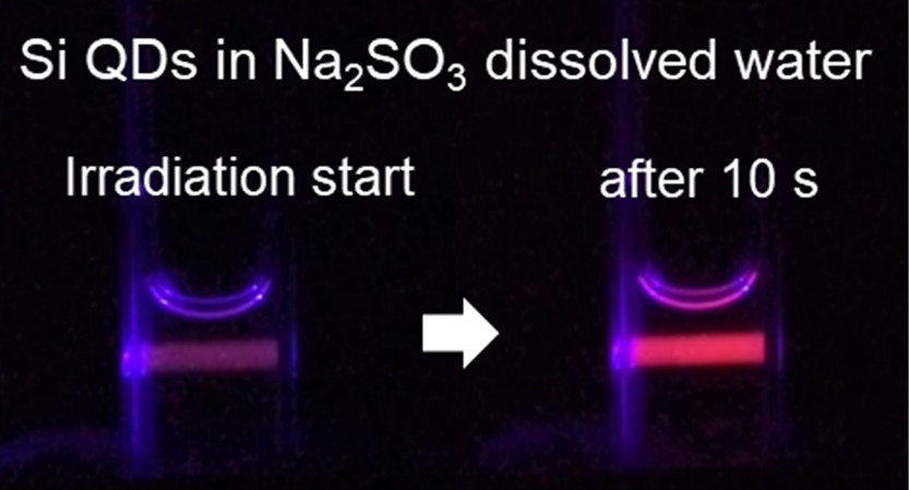 |
The effect of molecular reductants on the charge transfer-induced brightening of near-infrared photoluminescence (PL) from silicon (Si) quantum dots (QDs) was studied. Without a molecular reductant, a temporal decrease of the PL quantum yield (QY) during light irradiation in water was observed. The temporal photodarkening was reversed when a molecular reductant [sodium sulfites (Na2SO3)] was added in water. In Na2SO3-dissolved water, the PL QY increased gradually during light irradiation. The photobrightening behavior depended strongly on the amount of reductant molecules, excitation power, and the size of Si QDs. The observed phenomena suggest that an excess hole generated by trapping a photoexcited electron to a trap level is effectively removed by a reductant molecule. The observed charge transfer-induced photobrightening paves way to realize high efficiency and stable Si QDs-based phosphors usable in aqueous media. |
| 274. Eiji Takeda, Takehiro Zukawa, Tasuku Ishibashi, Kyohei Yoshino, Yukihiro Morita, and Minoru Fujii, "Mechanisms for the Degradation of Phosphor Excitation Efficiency by short wavelength vacuum ultraviolet Radiation in Plasma Discharge Devices", Journal of Physics and Chemistry of Solids, Vol. 124, pp. 274-280 (2019). (Available online 25 September 2018) | |
| The mechanism for the degradation of phosphor excitation efficiency in flat panel plasma discharge devices was investigated. We found that remaining organic compounds contained in the binders of phosphors were transformed to vacuum ultraviolet (VUV) absorbing substances over prolonged aging, which reduce the excitation efficiency of a phosphor, especially in the shorter wavelength VUV range. We also demonstrated that re-deposition of a sputtered protective layer on a phosphor further reduced the luminescence excitation efficiency due to the absorption of VUV radiation by the layer. | |
| 273. Byungjun Kang, Minoru Fujii, Dmitry Nesterenko, Zouheir Sekkat, and Shinji Hayashi, "Fano Resonances in Near-Field Absorption in All-Dielectric Multilayer Structures", Journal of Optics, Vol. 20, Issue 12, 125003, pp. 1-15 (2018). (Published 5 November 2018) | |
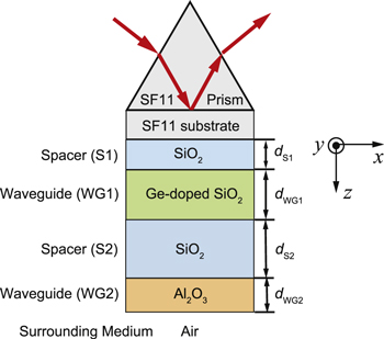 |
Extending our previous studies on metal-dielectric multilayer structures, we demonstrate thefeasibility of generating and controlling high-Q Fano resonances in all-dielectric multilayerstructures. The structures studied consist of two waveguide layers(Ge-doped SiO2and Al2O3layers)separated by spacer layers(SiO2layers)and arranged in the Kretschmann attenuated totalreflection geometry. From analyses based on the electromagnetic theory, we reveal that the Fanoresonance arises from the interaction between a broad waveguide mode supported by the Ge-doped SiO2layer and a sharp waveguide mode supported by the Al2O3layer. This mechanismallows us to generate similar Fano resonances with both thep- ands-polarized incident light.Although the Fano resonances based on radiative modes in a variety of nanostructures andmetamaterials have been reported to appear only in the far-field responses, we show that thepresent Fano resonances appear not only in the far-field reflection spectra but also in the near-field absorption spectra. |
| 272. Hiroshi Sugimoto, Masataka Yamamura, Riku Fujii, and Minoru Fujii, "Donor-Acceptor Pair Recombination in Size-Purified Silicon Quantum Dots", Nano Letters, Vol. 18, Issue 11, pp. 7282-7288 (2018). (Publication Date (Web): September 28, 2018) | |
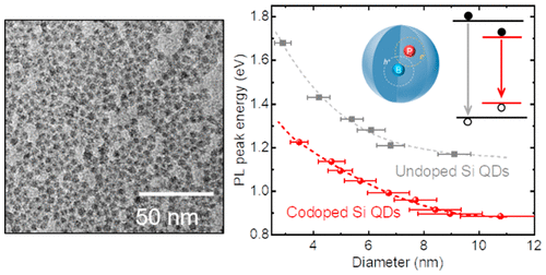 |
Shallow impurity doping is an efficient route to tailor optical and electronic features of semiconductor quantum dots (QDs). However, the effect of doping is often smeared by the size, shape, and composition inhomogeneities. In this paper, we study optical properties of almost monodispersed spherical silicon (Si) QDs that are heavily doped with boron (B) and phosphorus (P). The narrow size distribution achieved by a size-separation process enables us to extract doping-induced phenomena clearly. The degree of doping-induced shrinkage of the optical band gap is obtained in a wide size range. Comparison of the optical band gap with theoretical calculations allow us to estimate the number of active donor?acceptor pairs in a QD. Furthermore, we found that the size and detection energy dependence of the luminescence decay rate is significantly modified below a critical diameter, that is ?5.5 nm. In the diameter range above 5.5 nm, the luminescence decay rate is distributed in a wide range depending on the detection energy even in size-purified Si QDs. The distribution may arise from that of donor?acceptor distances. On the other hand, in the diameter range below 5.5 nm the detection energy dependence of the decay rate almost disappears. In this size range, which is smaller than twice of the effective Bohr radius of B and P in bulk Si crystal, the donor?acceptor distance is not a crucial factor to determine the recombination rate. |
| 271. Rens Limpens, Hiroshi Sugimoto, Nathan R Neale, and Minoru Fujii, "Critical Size for Carrier Delocalization in Doped Silicon Nanocrystals: A Study by Ultrafast Spectroscopy", ACS Photonics, Vol. 5, Issue 10, pp. 4037-4045 (2018). (Publication Date (Web): September 21, 2018) | |
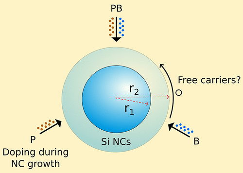 |
We present a comprehensive ultrafast spectroscopy-based study on the delocalization of doping-induced carriers in Si nanocrystals (NCs). To this end we prepare thin films of differently sized doped Si NCs and vary the doping configurations from singly P and B doping to simultaneously P and B co-doping. We show that the NC size orchestrates the level of delocalization of the doping-induced carriers. This can be understood in light of (1) the quantum confinement effect and (2) unscreened Coulomb interactions by moving further into the nanoscale. Both contributions affect the activation energy (ΔE) that is required to create free majority carriers. By varying the NC size in combination with the doping configuration we tune ΔE and control the delocalization of the doping-induced carriers. Most importantly, we show that there is a critical NC diameter of Dcritical ? 6 nm that describes the transition from a localized to a free carrier regime. In particular, our results show that optical bandgaps of ?0.95 eV (optimal for carrier multiplication-facilitated solar cell power conversion) can be achieved in P?B co-doped Si NCs with DNC < Dcritical. These results indicate that the practical photovoltaic feasibility of co-doped Si NCs is not limited by the presence of some remaining free carriers in uncompensated NCs. |
| 270. Shoya Takidani, Kanna Aoki, and Minoru Fujii, "One-step Discrete Symmetric Arrangement of Magnetic Micro Spheres with Nanoscale Spacing Immobilized by Ultraviolet Irradiation toward Plasmonic Resonators", ACS Applied Nano Materials, Vol. 1, Issue 11, pp. 6055-6062 (2018). (August 29, 2018) | |
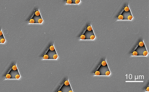 |
Micron-scale paramagnetic spheres are organized into discrete symmetric assemblies in a single step by overcoming the repulsive forces between them and balancing the magnetic attractive forces between the spheres and diamagnetic photoresist molds. Various symmetric arrangements of the spheres are obtained by modifying the shape and depth of the photoresist mold, the size of the spheres, and the magnetic susceptibilities of the paramagnetic spheres and the background medium. Permanent preservation of the assembled structure has been an issue for this type of assembly for years, because the magnetically assembled structures are maintained only under the external magnetic field. In this study, we overcome this issue by simple UV light irradiation during the magnetic assembly so that the surfaces of the sphere and substrate melt and fuse with each other, thus locking the position of the spheres on the substrate surface. This technique allowed permanent fixation of the symmetrically arranged paramagnetic spheres within 60 s, with the nanoscale spacings between adjacent spheres being maintained as narrow as 110 nm. This technique provides access to a wider variety of micro- and nanostructures and is thus useful in many research fields and industries. Particularly, such symmetric metal structures with nanogaps can serve as good media for plasmonic resonators. |
| 269. Akiko Minami, Hiroshi Sugimoto, Iain Crowe, and Minoru Fujii, "Growth of Core-Shell Silicon Quantum Dots in Borophosphosilicate Glass Matrix - Raman and Transmission Electron Microscopic Studies", The Journal of Physical Chemistry C, Vol. 122, Issue 36, pp. 21069-21075 (2018). (Publication Date (Web): August 22, 2018) | |
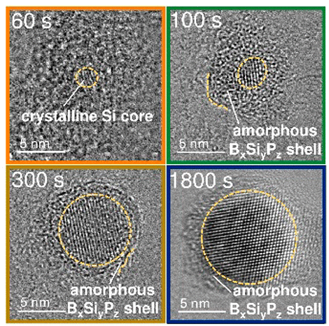 |
Annealing silicon- (Si-) rich borophosphosilicate glass (BPSG) at a high temperature results in the growth of core?shell Si quantum dots (QDs) composed of a boron (B) and phosphorus (P) codoped crystalline Si core and an amorphous shell made from B, Si, and P (B and P codoped Si QDs) in a BPSG matrix. The amorphous BxSiyPz shell is responsible for many superior properties of codoped Si QDs such as hydrophilicity, high resistance to hydrofluoric acid (HF) etching, stable luminescence in different environment, robustness of the luminescence for chemical treatments, etc. In this work, we study the growth process of the amorphous shell by Raman spectroscopy and transmission electron microscopy. We show that amorphous Si particles are first grown in a BPSG matrix within 30 s of annealing of Si-rich BPSG. After 50 s annealing, a crystalline Si core appears within an amorphous Si particle. The formation of a crystalline Si core is accompanied by the formation of an amorphous BxSiyPz shell. From the annealing time dependence of the volumes of the core and the shell, we show that supersaturated B and P are expelled to the surface of a crystalline Si core during the growth, which increases B and P concentration in an amorphous BxSiyPz shell. |
| 268. Shinya Kano, and Minoru Fujii, "All-Painting Process To Produce Respiration Sensor Using Humidity-Sensitive Nanoparticle Film and Graphite Trace", ACS Sustainable Chemistry & Engineering, Vol. 6, Issue 9, pp. 12217-12223 (2018). (Publication Date (Web): August 13, 2018) | |
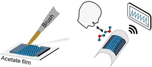 |
We propose an all-painting process to produce a respiration sensor made from a humidity-sensitive nanoparticle (NP) film and a graphite trace. The sensor is fabricated under ambient air with a simple vacuum-free process for green electronics: solely hand-painting on a cellulose acetate film. A humidity-sensitive silica NP film is painted by brush on pencil-trace graphite electrodes. An all-painted humidity sensor using this film shows 106% sensitivity within a 10?93% humidity change. The film is flexible and the humidity sensor operates as a respiration sensor after bending test. We design an all-painted respiration sensor using the humidity sensor and a painted resistor. Finally, we integrate the all-painted respiration sensor, a flexible temperature sensor, and a portable data logger as a portable bifunctional health-care device. The device on a mask can monitor human respiration rate and exhaled air temperature simultaneously. |
| 267. Takeshi Kawauchi, Shinya Kano, and Minoru Fujii, "Forming-Free Resistive Switching in Solution-Processed Silicon Nanocrystal Thin Film", Journal of Applied Physics, Vol. 124, 085113, pp. 1-6 (2018). (Published Online: 28 August 2018) | |
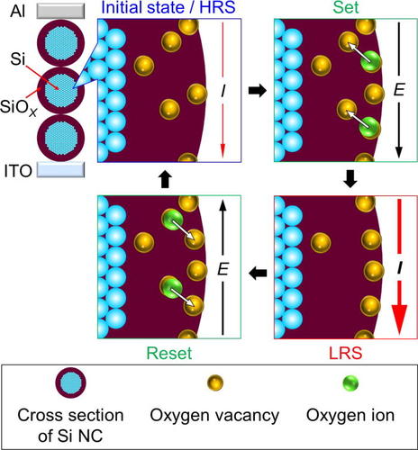 |
We report a forming-free resistive switching using a solution-processed silicon nanocrystal (Si NC) thin film. A Si NC thin film is formed on an ITO/glass substrate by spin-coating a colloidal Si NC solution in air. The Si NC thin film shows bipolar resistive switching without a forming process. Electrical characteristics at low temperatures and in various gas environments suggest that a non-stoichiometric SiOx shell on Si NCs contributes to the resistive switching. We propose that the origin of the resistive switching is a conductive filament of oxygen vacancies on the SiOx shell by an electric field. |
| 266. Tatsuki Hinamoto, Hiroshi Sugimoto, and Minoru Fujii, "Metal-Core/Dielectric-Shell/Metal-Cap Composite Nanoparticle for Upconversion Enhancement", The Journal of Physical Chemistry C, Vol. 122, Issue 30, pp. 17465-17472 (2018). (Publication Date (Web): July 12, 2018) | |
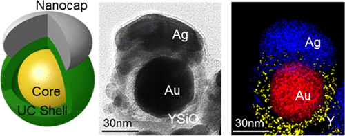 |
We have developed an upconversion composite nanoparticle composed of a metal core, an upconversion shell, and a metal cap. Numerical simulation of the nanocomposite revealed that hybridization of the localized surface plasmon modes of the core and the cap results in the emergence of novel bonding and antibonding modes. The latter mode has wide tunability in the resonance wavelength and strong field confinement at the position of the upconversion shell. For the fabrication of the composite nanoparticle, we developed a process that combines liquid-phase synthesis and vapor deposition processes. The scattering spectra of single composite nanoparticles agreed well with those in the numerical simulation. The comparison of the upconversion intensity between the metal-core/dielectric-shell structure and the metal-core/dielectric-shell/metal-cap structure revealed that the cap formation increases the intensity several folds. |
| 265. Makoto Sakiyama, Hiroshi Sugimoto, and Minoru Fujii, "Long-Lived Luminescence of Colloidal Silicon Quantum Dots for Time-Gated Fluorescence Imaging in the Second Near Infrared Window in Biological Tissue", Nanoscale, Vol. 10, Issue 29, pp. 13902-139007 (2018). (first published on 28 Jun 2018) | |
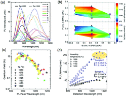 |
Boron (B) and phosphorus (P) codoped silicon quantum dots (Si QDs) are dispersible in polar solvents without organic ligands and exhibit photoluminescence (PL) in the first (NIR-I) and second (NIR-II) near infrared (NIR) windows in biological tissues due to the optical transition from the donor to acceptor states. We studied the relationship between the PL wavelength, lifetime and quantum yield (QY) of the colloidal solution and the composition of the starting material for the preparation. We found that the PL lifetime and the QY are primarily determined by the composition, while the PL wavelength is mainly determined by the growth temperature. By optimizing the composition, we achieved QYs of 20.1% and 1.74% in the NIR-I and NIR-II regions, respectively, in methanol. We demonstrate the application for time-gated imaging in the NIR-II range. |
| 264. Hiroshi Sugimoto, Shiho Yashima, and Minoru Fujii, "Hybridized Plasmonic Gap Mode of Gold Nanorod on Mirror Nanoantenna for Spectrally Tailored Fluorescence Enhancement", ACS Photonics, Vol. 5, Issue 8, pp 3421-3427 (2018). (Publication Date (Web): June 22, 2018) | |
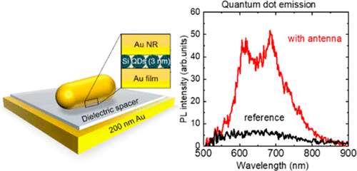 |
Plasmonic nanoparticle on mirror antennas with sub-10 nm gaps have shown the great potential in nanophotonic applications because they offer tightly confined electric field in the gap and resultant large Purcell factors. However, in a nanosphere on mirror (NSoM) structure being studied experimentally, the degree of freedom of the antennas in terms of spectral and polarization control is limited. In this work, we report spectral shaping and polarization control of Purcell-enhanced fluorescence by the gap plasmon modes of an anisotropic gold (Au) nanorod on a mirror (NRoM) antenna. Systematic numerical calculations demonstrate the richer resonance behaviors of a NRoM antenna than a NSoM antenna due to the hybridization of the bright and dark modes. We fabricate a NRoM antenna by placing a Au NR on an ultraflat Au film via a mono-, double-, or quadruple-layers of light emitting quantum dots (QDs) (3 nm in diameter). The scattering spectra of single NRoM antennas coincide very well with those of the numerical simulations. We demonstrate large enhancement (>900-fold) and strong shaping of the luminescence from QDs in the gap due to the coupling with the hybridized mode of a NRoM antenna. We also show that the polarization property of the emission is controlled by that of the mode coupled. |
| 263. Shinya Kano, Yasuhiro Tada, Satoshi Matsuda, and Minoru Fujii, "Solution Processing of Hydrogen-Terminated Silicon Nanocrystal for Flexible Electronic Device", ACS Applied Materials & Interfaces, Vol. 10, Issue 24, pp 20672-20678 (2018). (Publication Date (Web): May 29, 2018) | |
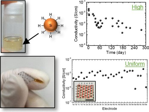 |
We demonstrate solution processing of hydrogen-terminated silicon nanocrystals (H?Si NCs) for flexible electronic devices. To obtain high and uniform conductivity of a solution-processed Si NC film, we adopt a perfectly dispersed colloidal H?Si NC solution. We show a high conductivity (2 × 10?5 S/cm) of a solution-processed H?Si NC film which is spin-coated in air. The NC film (area: 100 mm2) has uniform conductivity and responds to laser irradiation with 6.8 and 24.1 μs of rise and fall time. By using time-of-flight measurements, we propose a charge transport model in the H?Si NC film. For the proof-of-concept of this study, a flexible photodetector on a polyethylene terephthalate substrate is demonstrated by spin-coating colloidal H?Si NC solution in air. The photodetector can be bent in 5.9 mm bending radius at smallest, and the device properly works after being bent in 2500 cycles. |
| 262. Nguyen Xuan Chung, Rens Limpens, Chris de Weerd, Arnon Lesage, Minoru Fujii, and Tom Gregorkiewicz, "Towards practical carrier multiplication: Donor/acceptor co-doped Si nanocrystals in SiO2", ACS Photonics, Vol. 5, Issue 7, pp. 2843-2849 (2018). (Publication Date (Web): May 17, 2018) | |
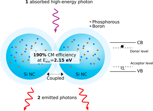 |
Carrier multiplication (CM) is an interesting fundamental phenomenon with application potential in optoelectronics and photovoltaics, and it has been shown to be promoted by quantum confinement effects in nanostructures. However, mostly due to the short lifetimes of additional electron?hole (e-h) pairs generated by CM, major improvements of quantum dot devices that exploit CM are limited. Here we investigate CM in SiO2 solid state dispersions of phosphorus and boron codoped Si nanocrystals (NCs): an exotic variant of Si NCs whose photoluminescence (PL) emission energy, the optical bandgap, is significantly red-shifted in comparison to undoped Si NCs. By combining the results obtained by ultrafast induced absorption (IA) with PL quantum yield (PL QY) measurements, we demonstrate CM with a long (around 100 μs) lifetime of the additional e-h pairs created by the process, similar as previously reported for undoped Si NCs, but with a significantly lower CM threshold energy. This constitutes a significant step toward the practical implementation of Si-based NCs in optoelectronic devices: we demonstrate efficient CM at the energy bandgap optimal for photovoltaic conversion. |
| 261. Minoru Fujii, Hiroshi Sugimoto, and Shinya Kano, "Silicon Quantum Dot with heavily Boron and Phosphorus Codoped Shell",Chemical Communications, Vol. 54, Issue 35, pp. 4375-4389 (2018). (First published on 30 Mar 2018) | |
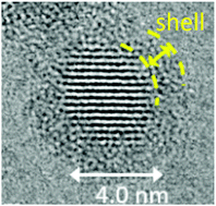 |
Heavily boron and phosphorus codoped silicon quantum dots (QDs) are dispersible in water without organic ligands and exhibit near infrared luminescence. We summarize the fundamental properties and demonstrate the formation of a variety of nanocomposites. |
| 260. Hiroshi Sugimoto, and Minoru Fujii, "Broadband Dielectric-Metal Hybrid Nanoantenna -Silicon Nanoparticle on Mirror", ACS Photonics, Vol. 5, Issue 5, pp. 1986-1993 (2018). (Publication Date (Web): March 23, 2018) | |
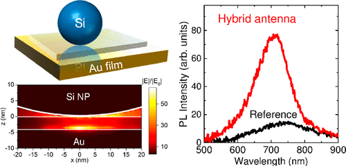 |
We developed a broadband dielectric-metal hybrid nanogap resonator composed of a silicon nanoparticle (Si NP) and gold (Au) flat surface. We fabricate the nanogap resonator by depositing a monolayer of colloidal quantum dots (QDs) (2.8 nm in diameter) on a Au surface followed by dropping a diluted colloidal solution of Si NPs (150 nm in diameter). The QD monolayer acts as a precisely length-controlled nanogap as well as a light emitter to monitor the radiative properties of the nanogap resonator. We investigate the light-scattering properties of single-nanogap resonators experimentally and theoretically and found that the coupling of the Mie resonance of Si NPs with a Au surface effectively confines the electromagnetic field into the nanogap in a wider wavelength range than an all-metal nanogap resonator with a comparable size. Furthermore, we show that the resonance wavelength of the hybrid nanogap resonator is less sensitive to the gap length than that of the all-metal one. We demonstrate that the broadband hybrid nanogap resonator enhances photoluminescence of a QD monolayer integrated in the nanogap by a factor of 786. |
| 259. Hiroshi Sugimoto, Masataka Yamamura, Makoto Sakiyama, and Minoru Fujii, "Visualizing Core-Shell Structure of Heavily Doped Silicon Quantum Dots by Electron Microscope using Atomically Thin Support Film", Nanoscale, Vol. 10, Issue 16, pp. 7357-7362 (2018). (First published on 21 Mar 2018) | |
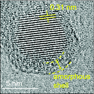 |
We successfully visualize a core?shell structure of a heavily B and P codoped Si quantum dot (QD) by transmission electron microscopy using an ultra-thin graphene oxide support film. The enhanced contrast reveals that a codoped Si QD has a highly crystalline Si core and an amorphous shell composed of Si, B and P. |
| 258. Byungjun Kang, Kenji Imakita, Minoru Fujii, and Shinji Hayashi, "Plasmonic Enhancement of Second-Harmonic Generation of Dielectric Layer Embedded in Metal-Dielectric-Metal Structure", Journal of Applied Physics, Vol. 123, Issue 12, pp. 123103-1-7 (2018). (Published Online: March 2018) | |
 |
The enhancement of second-harmonic generation from a dielectric layer embedded in a metal-dielectric-metal structure upon excitation of surface plasmon polaritons is demonstrated experimentally. The metal-dielectric-metal structure consisting of a Gex(SiO2)1-x layer sandwiched by two Ag layers was prepared, and the surface plasmon polaritons were excited in an attenuated total reflection geometry. The measured attenuated total reflection spectra exhibited two reflection dips corresponding to the excitation of two different surface plasmon polariton modes. Strong second-harmonic signals were observed under the excitation of these surface plasmon polariton modes. The results demonstrate that the second-harmonic intensity of the Gex(SiO2)1-x layer is highly enhanced relative to that of the single layer deposited on a substrate. Under the excitation of one of the two surface plasmon polariton modes, the estimated enhancement factor falls in a range between 39.9 and 171, while under the excitation of the other surface plasmon polariton mode, it falls in a range between 3.96 and 84.6. |
| 257. Yuki Ohata, Hiroshi Sugimoto, and Minoru Fujii, "Assembling Silicon Quantum Dots into Wires, Networks and Rods via Metal Ion Bridge ", Nanoscale, Vol. 10, Issue 16, pp. 7597-7604 (2018). (First published on 16 Mar 2018) | |
 |
Wires and networks of Si quantum dots (QDs) with a length of over 1 μm and a width of ?30 nm are produced by bridging Si QDs with metal ions in solution. It is shown that the width of the wires is almost independent of the preparation parameters and is always about 30 nm, except for the case when Si QDs larger than 30 nm are used, while the length of the wires depends strongly on the kinds of ions, the amount of ions and the amount of Si QDs in a solution. In addition to the microscopic size assemblies, macroscopic size rods of Si QDs with a width of ?20 μm are produced by using Zn2+ ions. The XPS analyses reveal that Si QDs are connected to each other via a ZnO layer in the rod. The rods have much higher conductivity and photo-response than Si QD solids produced without metal ions. |
| 256. Rens Limpens, Minoru Fujii, Nathan R. Neale, and Tom Gregorkiewicz, "Negligible Electronic Interaction between Photoexcited Electron-Hole Pairs and Free Electrons in Phosphorus-Boron Co-Doped Silicon Nanocrystals", The Journal of Physical Chemistry C, Vol. 122, Issue 11, pp. 6397-6404 (2018). (Publication Date (Web): March 5, 2018) | |
 |
Phosphorus (P) and boron (B) co-doped Si nanocrystals (NCs) have raised interest in the optoelectronic industry due to their electronic tunability, optimal carrier multiplication properties, and straightforward dispersibility in polar solvents. Yet a basic understanding of the interaction of photoexcited electron-hole (e-h) pairs with new physical features that are introduced by the co-doping process (free carriers, defect states, and surface chemistry) is missing. Here, we present the first study of the ultrafast carrier dynamics in SiO2-embedded P-B co-doped Si NC ensembles using induced absorption spectroscopy through a two-step approach. First, the induced absorption data show that the large fraction of the dopants residing on the NC surface slows down carrier relaxation dynamics within the first 20 ps relative to intrinsic (undoped) Si NCs, which we interpret as enhanced surface passivation. On longer time-scales (picosecond to nanosecond regime), we observe a speeding up of the carrier relaxation dynamics and ascribe it to doping-induced trap states. This argument is deduced from the second part of the study, where we investigate multiexciton interactions. From a stochastic modeling approach we show that localized carriers, which are introduced by the P or B dopants, have minor electronic interactions with the photoexcited e-h pairs. This is understood in light of the strong localization of the introduced carriers on their original P- or B-dopant atoms, due to the strong quantum confinement regime in these relatively small NCs (<6 nm). |
| 255. Takuya Kojima, Hiroshi Sugimoto, and Minoru Fujii, "Size-Dependent Photocatalytic Activity of Colloidal Silicon Quantum Dot", The Journal of Physical Chemistry C, Vol. 122, Issue 3, pp. 1874-1880 (2018). (Publication Date (Web): January 1, 2018) | |
 |
Photocatalytic activity of water-dispersible all-inorganic Si quantum dots (QDs) with heavily B and P codoped shells was studied by monitoring bleaching of Rhodamine B (RhB) in a mixture aqueous solution of Si QDs and RhB under light irradiation. The size of Si QDs was changed from 2.8 to 9.0 nm. A strong size dependence was observed in the dissociation rate of RhB. The observed size dependence of the rate could be well explained by the Marcus theory, which considers charge transfer from the LUMO of Si QDs to that of RhB. Quenching of the photoluminescence (PL) and the shortening of the PL lifetime of Si QDs due to the electron transfer to RhB were also observed. From these two approaches, we demonstrated that the quantum size effect plays a crucial role for the enhanced photocatalytic activity of Si QDs. |
| 254. Shinya Kano, Yuya Dobashi, and Minoru Fujii, "Silica Nanoparticle-Based Portable Respiration Sensor for Analysis of Respiration Rate, Pattern, and Phase during Exercise", IEEE Sensors Letters, Vol. 2, No 1, 2000104, pp. 1-4 (2018). (Date of Publication: 25 December 2017) | |
 |
We report a portable respiration sensor for the analysis of respiration rates, patterns, and phases during exercise. A silica nanoparticle thin film on a flexible substrate is used as a sensor chip (4.1 mm × 5 mm in area of electrodes) to detect respiration. Response and recovery time of the sensor chip are 0.7 and 1.7 s to detect human respiration. Even when it is covered with water, the response quickly recovers within 1 s after removal of the water. A portable respiration sensor can track respiration rates up to 1.7 Hz at rest. The sensor also monitors respiration patterns and phases during exercise noninvasively. The fast-response and portable respiration sensor is usable as a healthcare device. |
| 253. Hiroto Yanagawa, Asuka Inoue, Hiroshi Sugimoto, Masahiko Shioi, and Minoru Fujii, "Photoluminescence Enhancement of Silicon Quantum Dot Monolayer by Plasmonic Substrate Fabricated by Nano-Imprint Lithography", Journal of Applied Physics, Vol. 122, Issue , 22, pp. 223101-1-6 (2017). () |
|
 |
Near-field coupling between a silicon quantum dot (Si-QD) monolayer and a plasmonic substrate fabricated by nano-imprint lithography and having broad multiple resonances in the near-infrared (NIR) window of biological substances was studied by precisely controlling the QDs-substrate distance. A strong enhancement of the NIR photoluminescence (PL) of Si-QDs was observed. Detailed analyses of the PL and PL excitation spectra, the PL decay dynamics, and the reflectance spectra revealed that both the excitation cross-sections and the emission rates are enhanced by the surface plasmon resonances, thanks to the broad multiple resonances of the plasmonic substrate, and that the relative contribution of the two enhancement processes depends strongly on the excitation wavelength. Under excitation by short wavelength photons (405 nm), where enhancement of the excitation cross-section is not expected, the maximum enhancement was obtained when the QDs-substrate distance was around 30 nm. On the other hand, under long wavelength excitation (641 nm), where strong excitation cross-section enhancement is expected, the largest enhancement was obtained when the distance was minimum (around 1 nm). The achievement of efficient excitation of NIR luminescence of Si-QDs by long wavelength photons paves the way for the development of Si-QD-based fluorescence bio-sensing devices with a high bound-to-free ratio. |
| 252. Or Ashkenazi, Doron Azulay, Isaac Balberg, Shinya Kano, Hiroshi Sugimoto, Minoru Fujii, and Oded Millo,"Size-Dependent Donor and Acceptor States in Codoped Si Nanocrystals Studied by Scanning Tunneling Spectroscopy", Nanoscale, Vol. 9, Issue , , pp. 17884-17892 (2017). (first published on 06 Nov 2017
) |
|
 |
The electrical and optical properties of semiconductor nanocrystals (NCs) can be controlled, in addition to size and shape, by doping. However, such a process is not trivial in NCs due to the high formation energy of dopants there. Nevertheless, it has been shown theoretically that in the case of B and P (acceptor/donor) codoped Si-NCs the formation energy is reduced relative to that of single type doping. Previous comprehensive measurements on ensembles of such codoped Si-NCs have pointed to the presence of donor and acceptor states within the energy gap. However, such a conjecture has not been directly verified previously. Following that, we investigate here the electronic properties of B and P codoped Si-NCs via Scanning Tunneling Spectroscopy. We monitored the quantum confinement effect in this system, for which the energy gap changed from 1.4 eV to 1.8 eV with the decrease of NC diameter from 8.5 to 3.5 nm. Importantly, all spectra showed two in-gap band-states, one close to the conduction band edge and the other to the valence band edge, which we attribute to the P and B dopant levels, respectively. The energy separation between these dopants states decrease monotonically with increasing NC diameter, in parallel to the decrease of the conduction-to-valence bands separation. A fundamental quantity that is derived directly for these Si-NCs is the intrinsic like position of the Fermi energy, a non-trivial result that is very relevant for understanding the system. Following the above results we suggest an explanation for the character and the origin of the dopants bands. |
| 251. S. Hayashi, Y. Fujiwara, B. Kang, M. Fujii, D.V. Nesterenko, Z. Sekkat,"Line Shape Engineering of Sharp Fano Resonance in Al-Based Metal-Dielectric Multilayer Structure ", Journal of Applied Physics, Vol. 122, Issue 16, 163103, pp. 1-8 (2017). (Published Online: October 2017) |
|
 |
A systematic experimental study was performed on the Fano line shape exhibited by multilayer structures consisting of an Al layer, a SiO2 spacer layer, and an Al2O3 waveguide layer. In the structures studied, a sharp Fano resonance appears on the background of broad asymmetric resonance attributed to the excitation of a surface plasmon polariton at the Al/SiO2 interface. It is shown that the background asymmetric surface plasmon resonance can be well fitted to a single Fano function, and the sharp Fano line shape can be well fitted to a double Fano function expressed as a product of two single Fano functions. The results of measurements performed by varying the spacer layer thickness indicate that the width (Q factor) of the sharp Fano resonance decreases (increases) monotonously as the thickness increases. The Q factor achieved in the present study is as high as 1500. A comparison with the results of electromagnetic calculations suggests that not only the spacer layer thickness but also the imaginary part of the dielectric constant of the waveguide layer plays an important role in the Fano line shape engineering. |
| 250. Kanna Aoki, Keita Ishiguro, Masaki Denokami, Yuya Tanahashi, Kentaro Furusawa, Norihiko Sekine, Tadafumi Adschiri, and Minoru Fuji,"Direct Microrolling Processing on a Silicon Wafer", Small, Vol. 13, Issue 36, 1701630, pp. 1-8 (2017). (First published: 14 August 2017) |
|
 |
Although, varieties of micro‐ to nanoscale fabrication technologies have been invented and refined for silicon (Si) processing because Si is the basic material of integrated circuits, the layouts are based on layer‐by‐layer approaches, making it difficult to realize three‐dimensional (3D) structures with complicated shapes normal to the planar surface (along the out‐of‐plane direction) of the wafers used. Here, a novel and direct Si‐processing technology that enables to bend thin layers of Si surfaces into various 3D curved structures at the micrometer scale is introduced. This bending is achieved by porosifying a Si wafer surface using anodic oxidation and then performing conventional photolithography patterning and wet etching. The porosity gradient in the depth direction gives rise to a stress‐internalized layer in which self‐rolling action is induced via subsequent patterning and wet etching. A subsequent oxidation process further enhances the curvature deformation, leading to the formation of tubes, for example. The rolling directions can be controlled by 2D patterning of the porous Si layer, which is explained well from a structural dynamics perspective. This technology has a wide range of capabilities for realizing 3D structures on Si substrates, enabling new design possibilities for Si‐based on‐chip devices. |
| 249. A. Mazurak, R. Mroczynski, J. Jasinski, D. Tanous, B. Majkusiak, S. Kano, H. Sugimoto, M. Fujii, J. Valent,"Technology and Characterization of MIS Structures with Co-Doped Silicon Nanocrystals (Si-NCs) Embedded in Hafnium Oxide (HfOx) Ultra-Thin Layers", Microelectronic Engineering, Vol. 178, No. 25, pp. 298-303 (2017). (Available online 26 May 2017) |
|
 |
In this work, the technology of the metal-insulator-semiconductor (MIS) structures with co-doped silicon nanocrystals (Si-NCs) embedded in hafnium oxide (HfOx) dielectric layer is presented. The results of structural and electrical characterization of the fabricated test structures are discussed. A good agreement between measurements of thickness of the Si-NC layers for the spectroscopic ellipsometry and AFM methods was obtained. The spectroscopic analysis demonstrated a presence of Si-NCs of optical properties similar to the monocrystalline silicon. A simulation of the capacitance-voltage-time and current-voltage-time characteristics gave results of a qualitative agreement with the measurement data. Comparative stress-and-sense measurements (I-t) for the MIS structures with and without silicon nanocrystals proved the essential difference resulting from the charging/discharging processes of the nanocrystals. |
| 248. Shinya Kano, Kwangsoo Kim, and Minoru Fujii "Fast-Response and Flexible Nanocrystal-Based Humidity Sensor for Monitoring Human Respiration and Water Evaporation on Skin", ACS Sensors, Vol. 2, Issue. 6, pp. 828-833 (2017). (Publication Date (Web): May 24, 2017) |
|
 |
We develop a fast-response and flexible nanocrystal-based humidity sensor for real-time monitoring of human activity: respiration and water evaporation on skin. A silicon-nanocrystal film is formed on a polyimide film by spin-coating the colloidal solution and is used as a flexible and humidity-sensitive material in a humidity sensor. The flexible nanocrystal-based humidity sensor shows a high sensitivity; current through the nanocrystal film changes by 5 orders of magnitude in the relative humidity range of 8-83%. The response/recovery time of the sensor is 40 ms. Thanks to the fast response and recovery time, the sensor can monitor human respiration and water evaporation on skin in real time. Due to the flexibility and the fast response/recovery time, the sensor is promising for application in personal health monitoring as well as environmental monitoring. |
| 247. Hiroshi Sugimoto, and Minoru Fujii "Colloidal Dispersion of Sub-Quarter Micron Silicon Spheres for Low-Loss Antenna in Visible Regime", Advanced Optical Materials, Vol. 5,Issue 17, 1700332, pp. 1-8 (2017). (First published: 11 July 2017) |
|
 |
This work reports the development of an agglomeration‐free colloidal solution of silicon (Si) spheres exhibiting the electric and magnetic dipole Mie resonances in the visible region as an alternative to the optical nanoantenna based on plasmonic nanoparticles. Size‐controlled crystalline Si spheres with 20-250 nm in diameters are grown by a bottom‐up process. The Si spheres have heavily boron (B) and phosphorus (P) codoped surface layers, which induce negative surface potential and make the spheres dispersible in alcohol almost perfectly due to the electrostatic repulsions. Formation of agglomeration‐free colloidal dispersion allows to deposit Si spheres on an arbitrary substrate and to produce a dielectric nanoantenna for tailored wavelengths. This study demonstrates that, thanks to the almost perfect spherical shape of the developed Si spheres, the forward and backward scattering spectra of single Si spheres can be well‐explained by the Mie resonance in a wide size range. It is demonstrated that the Si spheres work as nanoantennas for fluorescence enhancement and a single Si sphere can enhance dye fluorescence at maximum 200‐fold. |
| 246. Hiroshi Sugimoto, Yusuke Ozaki, and Minoru Fujii "Silicon Quantum Dots in Dielectric Scattering Media-Broadband Enhancement of Effective Absorption Cross Section by Light Trapping", ACS Applied Materials & Interfaces, Vol. 9, Issue. 22, pp. 19135-19142
(2017). (Publication Date (Web): May 17, 2017) |
|
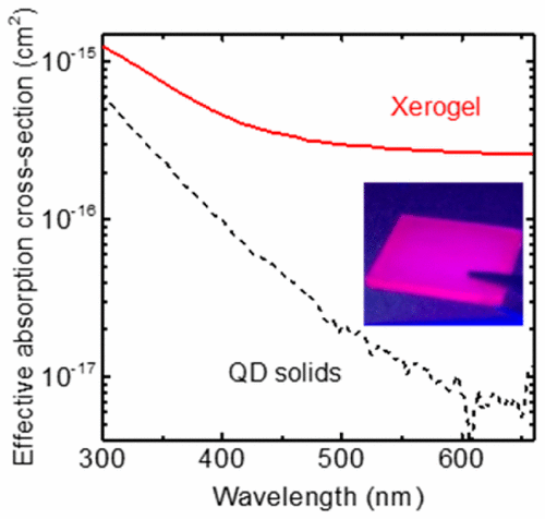 |
We report strong enhancements of the effective absorption cross section and photoluminescence (PL) intensity of silicon quantum dots (Si QDs) with 2.8-6.8 nm in diameter in a highly scattering dielectric medium. The scattering medium is a polymer thin film with submicrometer size pores inside, supporting the resonant cavity modes in the visible range. By the scattering associated with the cavity modes, efficient light trapping into a polymer film with ~1 μm in thickness is achieved, which leads to 30-40 times enhancement of the effective absorption cross section of embedded Si QDs in a green-red wavelength range. The scattering medium can also enhance up to 40 times the PL of QDs. Detailed analysis reveals that the enhancements of the extraction efficiency as well as the excitation efficiency contribute to the PL enhancement. |
| 245. Asuka Inoue, Hiroshi Sugimoto, and Minoru Fujii, "Photoluminescence Enhancement of Silicon Quantum Dot Monolayer by Double Resonance Plasmonic Substrate", The Journal of Physical Chemistry C, Vol. 121, Issue. 21, pp. 11609-11615 (2017). (Publication Date (Web): May 9, 2017) |
|
| A structure composed of a monolayer of luminescent silicon quantum dots (Si-QDs) and a silver (Ag) film over nanosphere (AgFON) plasmonic nanostructure is prepared by precisely controlling the distance. A AgFON structure modifies both the photoluminescence (PL) and the PL excitation (PLE) spectra of a Si-QD monolayer significantly. It is shown that the spectral shape is very sensitive to the spacer thickness and the wavelength dependence of the PL and PLE enhancement factors agrees well with the absorptance spectra. Due to multiple surface plasmon resonances of a AgFON structure, in proper spacer thicknesses, simultaneous enhancements of the excitation cross section and the emission rate are achieved. In the wavelength range where the absorption cross section of Si-QDs is small, the PL enhancement factor averaged in a relatively wide region (10 × 10 mm2) reaches 12. |
| 244. Hiroshi Sugimoto, Yusuke Hori, Yusuke Imura, and Minoru Fujii, "Charge Transfer Induced Photoluminescence Enhancement in Colloidal Silicon Quantum Dots", The Journal of Physical Chemistry C, Vol. 121, Issue. 21, pp. 11962-11967 (2017). (Publication Date (Web): May 8, 2017) |
|
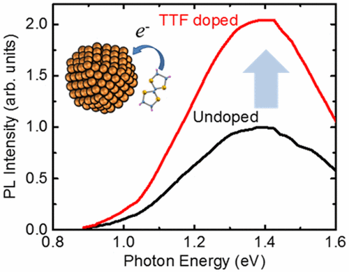 |
Charge transfer interaction between colloidal silicon (Si) quantum dots (QDs) and adsorbed molecules was investigated by means of photoluminescence (PL) spectroscopy. The molecule employed is tetrathiafulvalene (TTF), which has the highest occupied molecular orbital (HOMO) near that of Si QDs and can act as an electron donor to Si QDs. The energy difference between the HOMOs of TTF and Si QDs was controlled by changing the size of Si QDs. We found that the PL of Si QDs is strongly modified by the adsorption of TTF and that the PL change is reversible, that is, removal of TTF from a colloidal solution recovers the PL intensity. In the smallest Si QDs, where the HOMO level is expected to be 0.11 eV lower than that of TTF, a 2.5-fold enhancement of the PL was observed. The PL enhancement suggests that Si QDs having p-type behavior are compensated by electron transfer from TTF, similarly to the case of substitutional phosphorus doping in Si QDs. The observed size dependence of the PL enhancement factors suggests that the charge transfer process is described by classical Marcus theory. |
| 243. Tatsuki Hinamoto, Hiroshi Sugimoto, and Minoru Fujii, "Controlling Surface Plasmon Resonance of Metal Nanocap for Upconversion Enhancement", The Journal of Physical Chemistry C, Vol. 121, Issue. 14, pp. 8077-8083 (2017). (Publication Date (Web): March 29, 2017) |
|
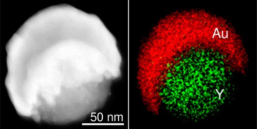 |
An upconversion composite nanoparticle (NP) composed of an Er and Yb doped Y2O3 (Y2O3:Yb,Er) NP and a Au nanocap was developed, and the effect of the coverage on the optical responses was studied by numerical simulations and optical measurements of single composite NPs. The formation of a composite NP and the control of the coverage were confirmed by transmission electron microscope observations. By controlling the coverage, the scattering peak due to the magnetic dipole surface plasmon resonance shifted from around 700 nm to over 900 nm. The upconversion intensity was also strongly modified by the coverage. Clear correlation was observed between the surface plasmon resonance wavelength and the upconversion intensity; the intensity increased as the resonance wavelength approached the excitation wavelength (975 nm). The largest enhancement factors of the upconversion with respect to that of a Y2O3:Yb,Er NP without a Au nanocap were 64 and 101-fold for the green (560 nm) and red (660 nm) emissions, respectively. |
| 242. Shinya Kano, and Minoru Fujii, "Conversion Efficiency of an Energy Harvester Based on Resonant Tunneling Through Quantum Dots with Heat Leakage", Nanotechnology, Vol. 28, No. 9, pp. 095403-1-7 (2017). (Published 31 January 2017) |
|
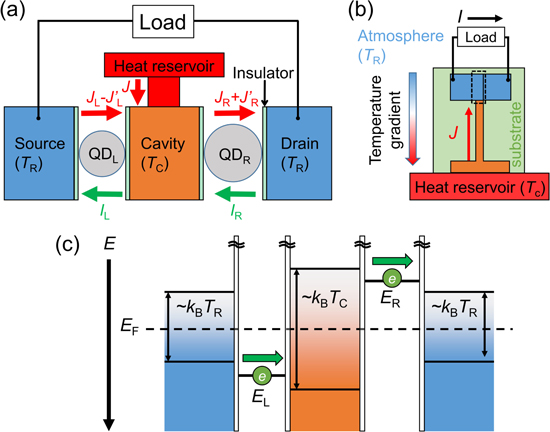 |
We study the conversion efficiency of an energy harvester based on resonant tunneling through quantum dots with heat leakage. Heat leakage current from a hot electrode to a cold electrode is taken into account in the analysis of the harvester operation. Modeling of electrical output indicates that a maximum heat leakage current is not negligible because it is larger than that of the heat current harvested into electrical power. A reduction of heat leakage is required in this energy harvester in order to obtain efficient heat-to-electrical conversion. Multiple energy levels of a quantum dot can increase the output power of the harvester. Heavily doped colloidal semiconductor quantum dots are a possible candidate for a quantum-dot monolayer in the energy harvester to reduce heat leakage, scaling down device size, and increasing electrical output via multiple discrete energy levels. |
| 241. Hui Lin, Kenji Imakita, Minoru Fujii, Chang Sun, Bingdi Chen, Takashi
Kanno, and Hiroshi Sugimoto, "New Insights into the Red Luminescent Bovine Serum Albumin Conjugated
Gold Nanospecies", Journal of Alloys and Compounds, Vol. 691, pp. 860-865 (2017). (Available online 30 August 2016) |
|
 |
Red luminescent bovine serum albumin conjugated gold nanospecies (BSA-Au) containing different total numbers of gold atoms and ions per one BSA molecule (AuTN/BSA) were synthesized. It is shown that pH has more influence on the emission properties than AuTN/BSA. pH sensitive and reversible emission variation (shift of the red emission peak wavelength, Δλ = 40 nm) was observed for the red emission from the BSA-Au samples. Together with the large Stokes shift in emission and the mixed singlet-triplet emission decay, it is suggested that the red emission from the BSA-Au samples agrees well with the features of metal-organic complexes. |
| 240. Shiho Yashima, Hiroshi Sugimoto, Hiroyuki Takashina, and Minoru Fujii, "Fluorescence Enhancement and Spectral Shaping of Silicon Quantum Dot Mono-Layer by Plasmonic Gap Resonances", The Journal of Physical Chemistry C, Vol. 120, Issue. 50, pp. 28795-28801 (2016). (Publication Date (Web): November 29, 2016) |
|
 |
A monolayer of silicon quantum dots (Si-QDs) 2.8 and 3.9 nm in diameter is placed in a gap between a gold (Au) thin film and a Au nanoparticle, and the photoluminescence (PL) properties are studied. By the metal nanoparticle over mirror (MNPoM) structure, the PL spectra of Si-QDs are strongly modified; the full width at half-maximum is reduced to 170 meV, which is less than half of that of Si-QDs on a silica substrate. The spectral shape coincides almost perfectly with that of the scattering spectrum of the MNPoM structure, indicating efficient coupling of the luminescence of Si-QDs with the gap surface plasmon modes. The luminescence intensity of Si-QDs in the gap is estimated to be enhanced about 700-fold compared to those on a Au film. |
| 239. Yasuhiro Higashikawa, Yasuo Azuma, Yutaka Majima, Shinya Kano, and Minoru Fujii, "Integration of Colloidal Silicon Nanocrystals on Metal Electrodes in Single-Electron Transistor", Applied Physics Letters, Vol. 109, Issue 21, 213104, pp. 1-5 (2016). (Published Online: November 2016) |
|
 |
We develop a facile process to integrate colloidal silicon nanocrystals (Si NCs) with metal electrodes in a single-electron transistor by self-assembly. Gold (Au) surface is modified by an amine-terminated self-assembled monolayer to have a positive potential. All-inorganic boron (B) and phosphorus (P) codoped Si NCs, with a negative surface potential and size-controllability, are selectively adsorbed on an amine-terminated Au surface by electrostatic attraction. We demonstrate the fabrication of SETs consisting of electroless-plated Au nanogap electrodes and codoped Si NCs using this process and observation of clear Coulomb diamonds at 9 K. |
| 238. Takashi Kanno, Shinya Kano, Hiroshi Sugimoto, Yasuhiro Tada, and Minoru
Fujii, "Water-Dispersible Near-Infrared Luminescent Silicon Nanocrystals-Immobilization
on Substrate", MRS Communications, Vol. 6, Issue 4, pp. 429-436 (2016). (Published online: 07 November 2016) |
|
 |
We demonstrate formation of allylamine (AAm) and acrylic acid (AAc)-functionalized colloidal silicon nanocrystals (Si NCs) exhibiting near-infrared (NIR) luminescence and immobilization of the NCs on substrates via covalent bond. The surface functionalization is confirmed by IR absorption spectroscopy and specific binding property of functionalized NCs. Atomic force microscope observations reveal that AAm- and AAc-functionalized Si NCs are chemically immobilized on self-assembled monolayers via covalent bonds. The functionalized Si NCs exhibit photoluminescence in a NIR region (1.5-1.6 eV), which is not significantly affected by the functionalization. |
| 237. Hiroshi Sugimoto, Kenta Furuta, and Minoru Fujii, "Controlling Energy Transfer in Silicon Quantum Dot Assemblies Made
from All-Inorganic Colloidal Silicon Quantum Dots", The Journal of Physical Chemistry C, Vol.120, Issue. 42, pp. 24469-24475 (2016).
(Publication Date (Web): October 10, 2016) |
|
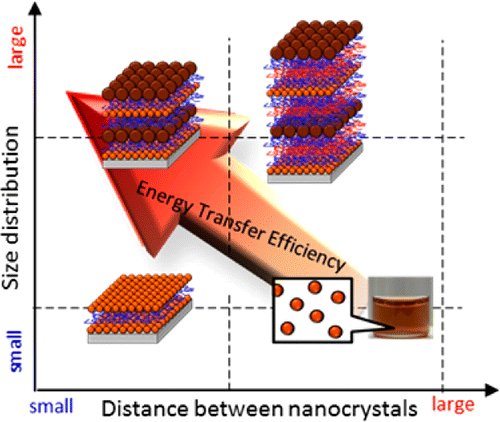 |
The optical response of an assembly of semiconductor quantum dots (QDs) is strongly modified from those of isolated ones by the inter-QD coupling. The strength of the coupling depends on the size, the inter-QD distance and the number of interacting QDs. In this work, we control these parameters of silicon (Si) QD assemblies by layer-by-layer growth of all-inorganic colloidal Si QDs. We perform detailed photoluminescence (PL) and PL decay dynamics studies for the assemblies made from monolayers of Si QDs 3.0 and 6.8 nm in diameters by precisely controlling the interlayer distance and the number of layers. From the analysis of the data with the Forster resonance energy transfer (FRET) model, we quantitatively discuss the relation between the FRET efficiency and the Forster radius in Si QD assemblies. |
| 236. Takashi Kanno, Hiroshi Sugimoto, Anna Fucikova, Jan Valenta, and Minoru
Fujii, "Single-Dot Spectroscopy of Boron and Phosphorus Codoped Silicon Quantum
dots", Journal of Applied Physics, Vol. 120, pp. 164307-1-6 (2016). (published online 27 October 2016) |
|
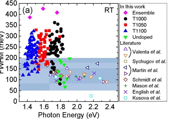 |
Boron (B) and phosphorous (P) codoped silicon quantum dots (Si QDs) are dispersible in polar solvents without organic ligands, and exhibit size controllable photoluminescence (PL) from 0.85 to 1.85 eV due to the electronic transitions between the donor and the acceptor states. We study the PL spectra of the codoped Si QDs at room temperature and at 77 K. We show that the broad PL band of codoped colloidal Si QDs (full width at half maximum is over 400 meV) is composed of narrower PL bands of individual QDs with different PL energies. We also show that the PL linewidth of individual codoped Si QDs is almost twice as large as those of undoped Si QDs. In contrast to the significant narrowing of the PL linewidth of undoped Si QDs at low temperatures, that of codoped Si QDs is almost independent of the temperature except for a few very small QDs. These results suggest that a large number of B and P are doped in a QD and there are a number of non-identical luminescence centers in each QD. |
| 235. Keita Nomoto, Hiroshi Sugimoto, Andrew Breen, Anna Ceguerra, Takashi
Kanno, Simon Ringer, Ivan Wurfl, Gavin Conibeer, and Minoru Fujii, "Atom Probe Tomography Analysis of Boron and/or Phosphorus Distribution
in Doped Silicon Nanocrystals", The Journal of Physical Chemistry C, Vol. 120, Issue 31, pp. 17845-17852 (2016).
(Publication Date (Web): July 27, 2016) |
|
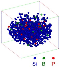 |
Silicon nanocrystals (Si NCs) are intensively studied for optoelectronic and biological applications due to having highly attractive features such as band engineering. Although doping is often used to control the optical and electrical properties, the related structural properties of solely doped and codoped Si NCs are not well-understood. In this study, we report the boron (B) and/or phosphorus (P) distribution in Si NCs embedded in borosilicate glass (BSG), phosphosilicate glass (PSG), and borophosphosilicate glass (BPSG) using atom probe tomography (APT). We compared solely and codoped Si NCs grown at different temperatures so that we may compare the effects of codoping and temperature on the B and/or P distribution. Proximity histograms and cluster analyses reveal that there exist boron-rich layers surrounding Si NCs and also B-P clusters within the Si NCs. Raman spectra also show a structural change between codoped Si NCs in solids and free-standing codoped Si NCs. These results lead us to understand that codoped Si NCs disperse in polar solvents. |
| 234. Asuka Inoue, Hiroshi Sugimoto, Hidenobu Yaku, and Minoru Fujii, "DNA Assembly of Silicon Quantum Dots / Gold Nanoparticle Nanocomposites",
RSC Advances, Vol. 6, Issue 68, pp. 63933-63939 (2016). (First published online 29 Jun 2016) |
|
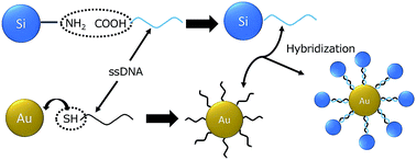 |
Silicon quantum dots (Si-QDs) dispersible in water and exhibiting bright near infrared (NIR) luminescence are a very attractive nano-light-emitter usable in bioimaging and biosensing. Here, we demonstrate the fabrication of NIR luminescent nanocomposites composed of Si-QDs and gold nanoparticles (Au-NPs) by DNA hybridization. We first develop processes to functionalize the surface of Si-QDs with different types of silane coupling agents without notably affecting the water solubility and the luminescence properties, and then conjugate the functionalized Si-QDs with single-stranded DNA (ssDNA). DNA hybridization with a Au-NP with complementary ssDNA results in the formation of Si-QDs/Au-NP nanocomposites. |
| 233. Lucie Ostrovska, Antonin Broz, Anna Fucikova, Tereza Belinova, Hiroshi
Sugimoto, Takashi Kanno, Minoru Fujii, Jan Valenta, and Marie Hubalek Kalbacova
, "The Impact of Doped Silicon Quantum Dots on Human Osteoblasts",
RSC Advances, Vol. 6, pp. 63403-63413 (2016). (First published online 28 Jun 2016) |
|
 |
Silicon (Si) nanostructures allow for the expansion of the application spectrum of this important semiconductor material with respect to the fields of optoelectronics and photonics. At the same time, the significant potential of Si quantum dots (SiQDs) has been revealed in terms of their potential application in the areas of biology and medicine due to their biocompatibility, low toxicity and natural biodegradability, unlike currently used semiconductor quantum dots. As far as this study is concerned, SiQDs co-doped with boron and phosphorus were used for the in vitro evaluation of their cytotoxicity in human osteoblasts. Two chemically identical types of SiQD differing in terms of their size and photoluminescence (PL) were studied. They both display long-lasting dispersion in methanol and even in aqueous media as well as PL which is not sensitive either to changes in the environment or surface modifications. Our experiments revealed significant differences between the two types of SiQD tested in regard to their behavior in a cell culture environment depending on increasing concentration (25-125 μg/ml) and cultivation conditions (the presence or absence of proteins from the fetal bovine serum - a component of the cultivation medium). A detailed description of their optical parameters and the evaluation of zeta potential enhance the understanding of the complexities of the in vitro results obtained. |
| 232. Hiroshi Sugimoto, Shiho Yashima, Kenta Furuta, Asuka Inoue, and Minoru
Fujii, "Probing Purcell Enhancement in Plasmonic Nanoantennas by Broadband
Luminescent Si Quantum Dots", Applied Physics Letters, Vol. 108, Issue 24, pp. 241103-1-4 (2016). (published online 14 June 2016) |
|
 |
Colloidal silicon quantum dots (Si QDs) with a very broad photoluminescence (PL) band are proposed as a probe to monitor the Purcell enhancement in a plasmonic nanostructure. Si QDs placed on an arbitrary plasmonic nanostructure enable us to determine the Purcell enhancement factors in a broad spectral range (600-900 nm). As a proof-of-concept experiment, a layer of Si QDs is spin-coated on gold film-over nanosphere structures, and the Purcell enhancement is quantitatively determined from the analyses of the PL spectra and the decay rates. The method proposed in this work provides a facile approach to quantitatively measure the performance of plasmonic substrates for PL and Raman enhancements. |
| 231. Shinya Kano, Masato Sasaki, and Minoru Fujii, "Combined Analysis of Energy Band Diagram and Equivalent Circuit on
Nanocrystal Solid", Journal of Applied Physics, Vol. 119, Issue 21, pp. 215304-1-6 (2016).
(Published online 3 June 2016) |
|
 |
We investigate a combined analysis of an energy band diagram and an equivalent circuit on nanocrystal (NC) solids. We prepared a flat silicon-NC solid in order to carry out the analysis. An energy band diagram of a NC solid is determined from DC transport properties. Current-voltage characteristics, photocurrent measurements, and conductive atomic force microscopy images indicate that a tunneling transport through a NC solid is dominant. Impedance spectroscopy gives an equivalent circuit: a series of parallel resistor-capacitors corresponding to NC/metal and NC/NC interfaces. The equivalent circuit also provides an evidence that the NC/NC interface mainly dominates the carrier transport through NC solids. Tunneling barriers inside a NC solid can be taken into account in a combined capacitance. Evaluated circuit parameters coincide with simple geometrical models of capacitances. As a result, impedance spectroscopy is also a useful technique to analyze semiconductor NC solids as well as usual DC transport. The analyses provide indispensable information to implement NC solids into actual electronic devices. |
| 230. Minoru Fujii, Hiroshi Sugimoto, and Kenji Imakita, "All-Inorganic Colloidal Silicon Nanocrystals-Surface Modification
by Boron and Phosphorus Co-Doping", Nanotechnology, Vol. 27, Issue 26, pp. 262001-1-20 (2016). (Published 18 May 2016 ) |
|
 |
Si nanocrystals (Si-NCs) with extremely heavily B- and P-doped shells are developed and their structural and optical properties are studied. Unlike conventional Si-NCs without doping, B and P co-doped Si-NCs are dispersible in alcohol and water perfectly without any surface functionalization processes. The colloidal solution of co-doped Si-NCs is very stable and no precipitates are observed for more than 5 years. The co-doped colloidal Si-NCs exhibit size-controllable photoluminescence (PL) in a very wide energy range covering 0.85 to 1.85 eV. In this paper, we summarize the structural and optical properties of co-doped Si-NCs and demonstrate that they are a new type of environmentally-friendly nano-light emitter working in aqueous environments in the visible and near infrared (NIR) ranges. |
| 229. Hiroshi Sugimoto, Kenji Imakita, and Minoru Fujii, "Silicon Nanocrystal-Noble Metal Hybrid Nanoparticles", Nanoscale, Vol. 8, Issue 21, pp. 10956-10962 (2016). (First published online 13 Apr 2016) |
|
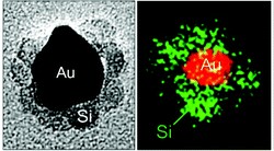 |
We report a novel and facile self-limiting synthesis route of silicon nanocrystal (Si NC)-based colloidally stable semiconductor-metal (gold, silver and platinum) hybrid nanoparticles (NPs). For the formation of hybrid NPs, we employ ligand-free colloidal Si NCs with heavily boron (B) and phosphorus (P) doped shells. By simply mixing B and P codoped colloidal Si NCs with metal salts, hybrid NPs consisting of metal cores and Si NC shells are spontaneously formed. We demonstrate the synthesis of highly uniform and size controllable hybrid NPs. It is shown that codoped Si NCs act as a reducing agent for metal salts and also as a protecting layer to stop metal NP growth. The process is thus self-limiting. The development of a variety of Si NC-based hybrid NPs is a promising first step for the design of biocompatible multifunctional NPs with broad material choices for biosensing, bioimaging and solar energy conversion. |
| 228. Valentin Nikolaev, Nikita Averkiev, and Minoru Fujii, "Phenomenological Theory of Optical Broadening in Zero-Dimensional
Systems Applied to Silicon Nanocrystals", Applied Physics Letters, Vol. 108, Issue 15, 153107 pp. 1-4 (2016). () |
|
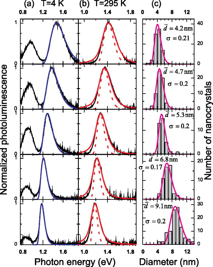 |
We develop a phenomenological theory of inhomogeneous broadening in zero-dimensional systems and apply it to study photoluminescence (PL) spectra of silicon nanocrystals measured at helium and room temperatures. The proposed approach allowed us to explain experimentally observed PL peak asymmetry, linear dependence of the peak width on its maximum, and anomalous alteration of spectral characteristics with temperature increase. |
| 227. Yusuke Hori, Shinya Kano, Hiroshi Sugimoto, Kenji Imakita, and Minoru
Fujii, "Size-Dependence of Acceptor and Donor Levels of Boron and Phosphorus
Codoped Colloidal Silicon Nanocrystals", Nano Letters, Vol. 16, Issue 4, pp. 2615-2620 (2016). (Publication Date (Web): March 21, 2016) |
|
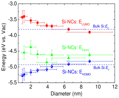 |
Size dependence of the boron (B) acceptor and phosphorus (P) donor levels of silicon (Si) nanocrystals (NCs) measured from the vacuum level was obtained in a very wide size range from 1 to 9 nm in diameter by photoemission yield spectroscopy and photoluminescence spectroscopy for B and P codoped Si-NCs. In relatively large Si-NCs, both levels are within the bulk Si band gap. The levels exhibited much smaller size dependence compared to the valence band and conduction band edges. The Fermi level of B and P codoped Si-NCs was also studied. It was found that the Fermi level of relatively large codoped Si-NCs is close to the valence band and it approaches the middle of the band gap with decreasing the size. The results suggest that below a certain size perfectly compensated Si-NCs, that is, Si-NCs with exactly the same number of active B and P, are preferentially grown, irrespective of average B and P concentrations in samples. |
| 226. Antonio J. Almeida, Hiroshi Sugimoto, Minoru Fujii, Martin S. Brandt,
Martin Stutzmann, and Rui N. Pereira, "Doping Efficiency and Confinement of Donors in Embedded and Free Standing Si Nanocrystals", Physical Review B, Vol. 93, Issue 11, 115425 pp. 1-9 (2016). (Published 17 March 2016) |
|
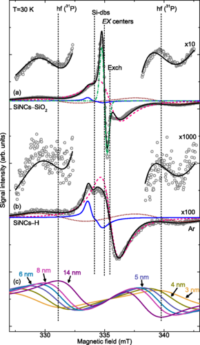 |
Doping semiconductor nanocrystals (NCs) is a promising way to tailor the optical and electronic behavior of these materials to enable their use in (opto)electronic applications. Yet the practical exploitation of doping requires an understanding of its efficiency, and dependence on external environment, and of the electronic localization of dopant states due to confinement effects. Here, we experimentally probe the efficiency of doping of Si NCs grown in amorphous SiO2 by means of phase segregation method. We estimate a P doping efficiency of these Si NCs of about 30% and from this we infer that most P dopants are incorporated at substitutional sites of the NCs lattice and thus act as donors. We further show that the doping efficiency in Si NCs varies by several orders of magnitude depending on their external environment. Charge traps associated with air molecules adsorbed to the NCs surface give rise to a strong compensation of donors. We observe that this process can be reverted by desorbing the molecules from the NCs surface under vacuum. Moreover, we experimentally assess the confinement energy of isolated donors in Si NCs from the temperature dependence of their magnetic resonance. From this, we provide experimental evidence for the confinement-induced increase of ionization energy of dopants with decreasing NC size previously predicted with ab initio calculations of doped Si NCs. |
| 225. Ramesh Ghosh, Kenji Imakita, Minoru Fujii and P. K. Giri, "Effect of Ag/Au Bilayer Assisted Etching on the Strongly Enhanced
Photoluminescence and Visible Light Photocatalysis from Si Nanocrystal
Decorated Si Nanowires Array", Physical Chemistry Chemical Physics, Vol. 18, pp. 7715-7727 (2016). (First published online 10 Feb 2016) |
|
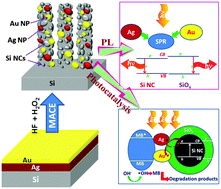 |
We report on the strongly enhanced photoluminescence (PL) and visible light photocatalysis by arrays of vertically aligned single crystalline Si nanowires (NWs) grown by Ag/Au bilayer assisted etching. High resolution FESEM and TEM imaging reveals that the Si NWs are decorated with ultra-small size arbitrary shaped Si nanocrystals (NCs) due to the lateral etching of the NWs. A strong broad band and tunable visible to near-infrared (NIR) photoluminescence (PL) in the range 1.3-2.4 eV are observed for these Si NWs/NCs at room temperature, depending on the etching conditions. Our studies reveal that the visible-NIR PL intensity is about two orders of magnitude higher and it exhibits faster decay dynamics in the bilayer assisted etching case as compared to the Ag or Au single layer etching case. The enhanced PL in the bimetal case is attributed to the longer length and higher density of the Si NWs/NCs, surface plasmon resonance enhanced absorption by residual bimetal NPs and the enhanced radiative recombination rate. Studies on the time evolution of PL spectral features with laser exposure under ambient conditions and laser power dependence reveal that both the quantum confinement of carriers in Si NCs and the nonbridging oxygen hole defects in the SiOx layer contribute to the tunable PL. Interestingly, Si NWs grown by Ag/Au bilayer assisted etching exhibit enhanced photocatalytic degradation of methylene blue in comparison to Si NWs grown by single layer Ag or Au assisted etching. The Schottky barrier present between bimetallic NPs and nanoporous Si NWs with Si-H bonds facilitates the photocatalytic activity by efficient separation of photogenerated e-h pairs. Our results demonstrate the superiority of the Si NW array grown by bilayer assisted etching for their cutting edge applications in optoelectronics and environmental cleaning. |
| 224. Masato Sasaki, Shinya Kano, Hiroshi Sugimoto, Kenji Imakita, and Minoru
Fujii, "Surface Structure and Current Transport Property of Boron and Phosphorous
Co-doped Silicon Nanocrystals", The Journal of Physical Chemistry C, Vol. 120, Issue. 1, pp. 195-200 (2016).
(Publication Date (Web): December 8, 2015) |
|
 |
Silicon (Si) nanocrystals (NCs) with high boron (B) and phosphorus (P) concentration shells are dispersible in polar solvents without organic ligands. In order to understand the mechanism of the solution dispersibility, the surface structure is studied by infrared absorption spectroscopy. It is shown that water molecules are adsorbed at the B-oxygen (O) bond sites on NC surface with high hydrogen bond strength, and thus B and P co-doped Si-NCs are a kind of hydrate containing large amounts of water molecules (Si-NC・xH2O). The current transport properties of Si-NC films made from the solutions are studied. It is found that the conductivity is very sensitive to the amount of adsorbed water molecules and changes by 8 orders of magnitude. The high affinity of the NC surface with water molecules is considered to be the origin of the high sensitivity. |
| 223. Batakrushna Santara, Kenji Imakita, Minoru Fujii, and P. K. Giri,
"Mechanism of Defects Induced Ferromagnetism in Undoped and Cr Doped
TiO2 Nanorods/Nanoribbons", Journal of Alloys and Compounds, Vol. 661, pp. 331-344 (2016). (Published 15 March 2016) |
|
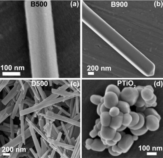 |
We have studied the effect of doping concentrations, growth temperature and calcinations on the structural, optical and magnetic properties of the undoped and Cr doped TiO2 nanorods/nanoribbons (NR/NRb), in order to develop an improved understanding on the mechanism of room temperature (RT) ferromagnetism (FM) in these nanostructures. Both undoped and doped TiO2 NR/NRb exhibit RT FM and a ~2.6 fold enhancement in magnetization is observed in 0.3% Cr doped TiO2 NR/NRb as compared to the undoped NR/NRb, and the magnetization increases considerably after vacuum annealing. However, no measureable FM is observed for the precursor TiO2 powder, despite the presence of high concentration of oxygen vacancies in it. On the other hand, the magnetization decreases at higher doping concentration (0.7% Cr) as compared to 0.3% Cr doped sample. Thus, our studies revealed that a simple oxygen vacancy and/or Cr ions alone cannot yield the RT FM in TiO2 nanostructures. We argue that the oxygen vacancy with appropriate charge redistribution and their orbital overlapping, and exchange interaction with the nearby unpaired 3d electron of Ti3+ in undoped TiO2 and/or unpaired 3d electrons of Cr3+ dopant with proper charge distribution and occupation inside the host lattice in Cr doped TiO2 nanostructures play the pivotal role for the ferromagnetic ordering and observed RTFM. The presence of oxygen vacancy related F+-center and Cr3+ are confirmed from the electron spin resonance and x-ray photoelectron spectroscopy measurements. |
| 222. Hiroshi Sugimoto, Kenji Imakita and Minoru Fujii "Growth of Novel Boron-Rich Nanocrystals from Oxygen-Deficient Borophosphosilicate Glasses for Boron Neutron Capture Therapy", RSC Advances, Vol. 5, Issue 119, pp. 98248 - 98253 (2015). (First published online 17 Nov 2015) |
|
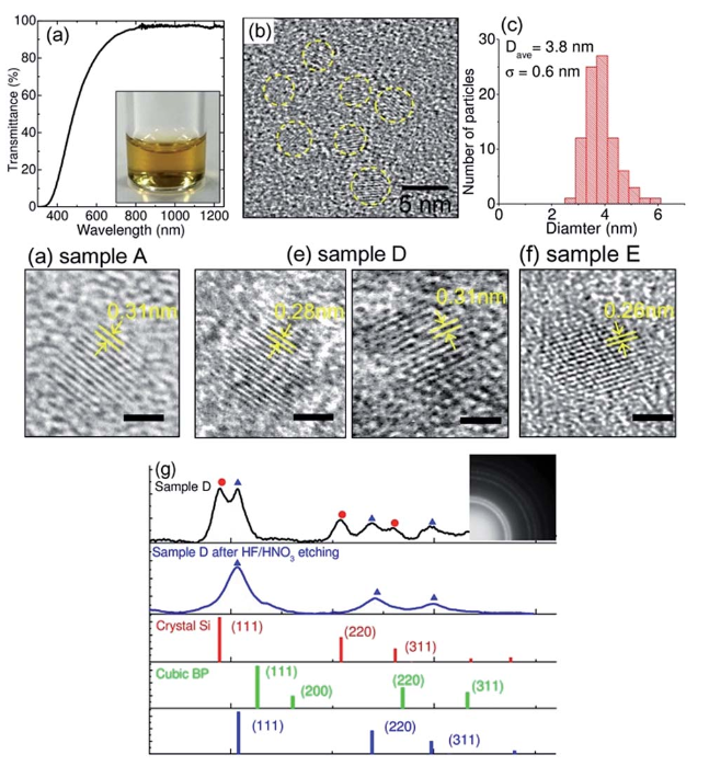 |
We develop a new type of boron (B)-rich nanocrystals (NCs) for applications in Boron Neutron Capture Therapy (BNCT). Phase separation of oxygen (O) deficient borophosphosilicate glasses (BPSG) by annealing in inert ambient gas results in the growth of different types of B-rich NCs. When the silicon (Si) concentration is much higher than the others, B and phosphorus (P) co-doped Si-NCs are grown. In the opposite case, cubic boron phosphide (BP) NCs are grown. In between two extremes, we demonstrate the growth of a new type of cubic NCs consisting of B, Si and P with an average B concentration up to 36 at%. The B-rich NCs are dispersible in water and exhibit photoluminescence in the biological window. These properties in combination with the capability of the bio-functionalization via the surface Si-hydrogen (H) and Si-O bonds suggest that the B-rich NCs can be a multifunctional biomaterial used for imaging, diagnosis and BNCT. |
| 221. Rens Limpens, Arnon Lesage, Minoru Fujii, and Tom Gregorkiewicz "Size Confinement of Si Nanocrystals in Multinanolayer Structures", Scientific Reports, Vol. 5, No. 17289, pp. 1-6 (2015). (Published: 25 November 2015) |
|
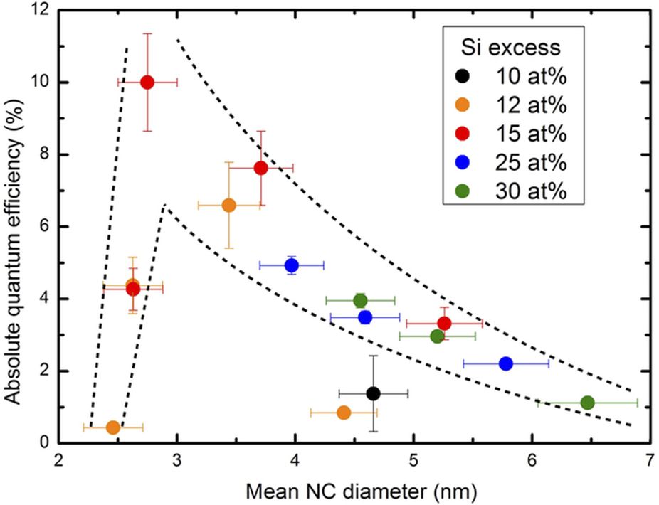 |
Si nanocrystals (NCs) are often prepared by thermal annealing of multiple stacks of alternating sub-stoichiometric SiOx and SiO2 nanolayers. It is frequently claimed that in these structures, the NC diameter can be predefined by the thickness of the SiOx layer, while the NC concentration is independently controlled by the stoichiometry parameter x. However, several detailed structural investigations report that the NC size confinement to within the thickness of the SiOx layer is not strictly obeyed. In this study we address these contradicting findings: based on cross-correlation between structural and optical characterization of NCs grown in a series of purposefully prepared samples of different stoichiometry and layer thickness, we develop a comprehensive understanding of NC formation by Si precipitation in multinanolayer structures. We argue that the narrow NC size distribution generally observed in these materials appears due to reduction of the Si diffusion range, imposed by the SiO2 spacer layer. Therefore, both the SiOx layer thickness and composition as well as the actual thickness of the SiO2 spacer play an essential role in the NC formation. |
| 220. Asuka Inoue, Minoru Fujii, Hiroshi Sugimoto, and Kenji Imakita "Surface Plasmon-Enhanced Luminescence of Silicon Quantum Dots in Gold Nanoparticle Composites", The Journal of Physical Chemistry C, Vol. 119, Issue. 44, pp. 25108-25113 (2015). (Publication Date (Web): October 13, 2015) |
|
 |
A composite nanoparticle (NP) consisting of a gold nanoparticle (Au-NP) core and a thick shell of silicon quantum dot (Si-QD) agglomerates was developed. In the composite NPs with an optimized amount of Si-QDs per a Au-NP, photoluminescence from Si-QDs was enhanced, when it was excited in the wavelength range of the localized surface plasmon resonances (LSPRs) of Au-NPs. The experimental results could be well-explained by a simple model consisting of a spherical Au-NP and a spherical shell made from Si-QD aggregates. It was found that the enhancement is due to increased excitation efficiency of Si-QDs via the LSPR of Au-NPs. |
| 219.Hui Lin, Kenji Imakita, Minoru Fujii, V. Yu. Prokof'ev, N. E. Gordina,
B. Said, and A. Galarneau "Visible Emission from Ag+ Exchanged SOD Zeolites", Nanoscale, Vol. 7, Issue 38, pp. 15665-15671 (2015). (First published online 09 Sep 2015) |
|
 |
Broad visible emissions dominant at green or red have been observed for the thermally-treated Ag+ exchanged SOD zeolites, determined by the Ag+ loading contents and the excitation wavelengths. Contrary to the notable reversible green/red dominant emission evolution in the Ag+ exchanged LTA zeolites upon hydration/dehydration in air (or water vapor)/vacuum, emission spectra of the Ag+ exchanged SOD zeolites are insensitive to the environmental change. This is most probably due to the difficult H2O permeation in SOD zeolites in comparison with LTA zeolites. By combining the environment dependent emission spectra of the Ag+ exchanged LTA and SOD zeolites, we proposed the following emission mechanisms for Ag+ exchanged LTA and SOD zeolites: the green emission is due to the transition from ligand-to-metal (framework O2 → Ag+) charge transfer state to the ground state and the red emission is due to the transition from the metal-metal (Ag+-Ag+) charge transfer state to the ground state. The insensitive environment dependent emission characteristics of Ag+ exchanged SOD zeolites may have potential applications as robust phosphors. |
| 218. Hiroshi Sugimoto, Tianhong Chen, Ren Wang, Minoru Fujii, Bjoern M.
Reinhard, and Luca Dal Negro "Plasmon-Enhanced Emission Rate of Silicon Nanocrystals in Gold Nanorod Composites", ACS Photonics, Vol. 2, Issue. 9, pp. 1298-1305 (2015). (Publication Date (Web): August 4, 2015) |
|
 |
We develop colloidal nanocomposites consisting of coupled light-emitting Si nanocrystals (NCs) and Au nanorods and systematically investigate their structural and photoluminescence (PL) properties, which demonstrate significant enhancement of spontaneous emission rate with suppressed nonradiative quenching. In addition, through a comparison of the polarization dependence of PL and scattering intensities of single nanocomposites, we successfully demonstrate that the emission from Si NCs coupled to Au nanorods is highly polarized along the major axis of nanorods. The experimental results in combination with rigorous simulations of dipolar emission in the vicinity of Au nanorods enable us to demonstrate a 3 times enhancement of the quantum efficiency at the peak of the NC emission. The Si-based active plasmonic-coupled nanocomposites developed in this work provide novel opportunities for biocompatible platforms that leverage nanoscale fluorescent probes for biosensing and bioimaging device applications. |
| 217. Rens Limpens, Arnon Lesage, Peter Stallinga, Alexander N. Poddubny,
Minoru Fujii, and Tom Gregorkiewicz "Resonant Energy Transfer in Si NC Solids", The Journal of Physical Chemistry C, Vol. 119, Issue. 33, pp. 19565-19570 (2015). (Publication Date (Web): July 27, 2015) |
|
 |
Energy exchange between closely packed semiconductor quantum dots allows for long-range transfer of electronic energy and enables new functionalities of nanostructured materials with a huge application potential in photonics, optoelectronics, and photovoltaics. This is illustrated by impressive advances of quantum-dot solids based on nanocrystals (NCs) of direct bandgap materials, where this effect has been firmly established. Regretfully, the (resonant) energy transfer in close-packed ensembles of NCs remains elusive for silicon the main material for electronic and photovoltaic industries. This is the subject of the present study in which we conclusively demonstrate this process taking place in dense dispersions of Si NCs in an SiO2 matrix. Using samples with different NC configurations, we can directly determine the wavelength dependent energy transfer rate and show that it (i) can be modulated by material parameters, and (ii) decreases with the NCs size, and thus being consistent with the energy flow proceeding from smaller to larger NCs. This result opens the way to new applications of Si NCs, requiring energy transport and extraction. In particular, it forms a fundamental step toward development of an excitonic all-Si solar cell, operating in some analogy to polymer devices. |
| 216. Hiroshi Sugimoto, Ran Zhang, Bjorn M. Reinhard, Minoru Fujii, Giovanni
Perotto, Benedetto Marelli, Fiorenzo G. Omenetto and Luca Dal Negro "Enhanced Photoluminescence of Si Nanocrystals-Doped Cellulose Nanofibers by Plasmonic Light Scattering", Applied Physics Letters, Vol. 107, Issue. 4, 041111 pp. 1-4 (2015). (published online 28 July 2015) |
|
 |
We report the development of bio-compatible cellulose nanofibers doped with light emitting silicon nanocrystals and Au nanoparticles via facile electrospinning. By performing photoluminescence (PL) spectroscopy as a function of excitation wavelength, we demonstrate plasmon-enhanced PL by a factor of 2.2 with negligible non-radiative quenching due to plasmon-enhanced scattering of excitation light from Au nanoparticles to silicon nanocrystals inside the nanofibers. These findings provide an alternative approach for the development of plasmon-enhanced active systems integrated within the compact nanofiber geometry. Furthermore, bio-compatible light-emitting nanofibers prepared by a cost-effective solution-based processing are very promising platforms for biophotonic applications such as fluorescence sensing and imaging. |
| 215. Ibuki Kawamura, Kenji Imakita, Akihiro Kitao, and Minoru Fujii, "Second-Order Nonlinear Optical Behavior of Amorphous SiOx Thin Films Grown by Sputtering", Journal of Physics D: Applied Physics, Vol. 48, No. 39, 395101 pp. 1-9 (2015). (Published 4 September 2015) |
|
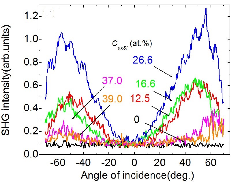 |
Second harmonic generation from amorphous SiO x thin films prepared by sputtering was investigated under a nanosecond pulse excitation at 1064?nm. The investigation over a wide range of preparation conditions, i.e. excess Si concentration (C exSi) and annealing temperature, revealed that the effective second-order nonlinear optical coefficient (d eff) reaches up to 0.59 pm V?1, which is comparable to that of α-quartz. The origin was discussed based on the results of x-ray photoelectron spectroscopy, electron spin resonance spectroscopy, and photoluminescence spectroscopy. A correlation was found between the ratio of d eff to C exSi and the peak energy of the photoluminescence, suggesting that Si clusters are the most probable origin of the second-order nonlinearity. |
| 214. Kenta Furuta, Minoru Fujii, Hiroshi Sugimoto, and Kenji Imakita "Energy Transfer in Silicon Nanocrystal Solids Made from All-Inorganic Colloidal Silicon Nanocrystals", The Journal of Physical Chemistry Letters, Vol. 6, Issue 14, pp. 2761-2766 (2015). (Publication Date (Web): June 25, 2015) |
|
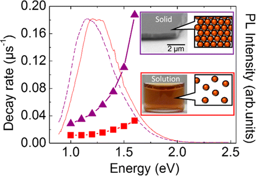 |
Energy transfer between silicon (Si) nanocrystals (NCs) in Si-NC solids was demonstrated by photoluminescence (PL) spectroscopy. Clear differences of PL spectra and the decay rates between solutions and solids of Si-NCs were observed. The change in the PL properties caused by the formation of solids could be explained by the energy transfer from small to large NCs in the size distribution. In order to obtain further evidence of NC-to-NC energy transfer, the size distribution was intentionally modified by mixing solutions of NCs with different size distributions. NC solids made from the mixed solutions exhibited significantly different PL spectral shape and decay rates from those made from unmixed solutions, providing clear evidence of NC-to-NC energy transfer in Si-NC solids. |
| 213. Yu Wang, Hiroshi Sugimoto, Sandeep Inampudi, Antonio Capretti, Minoru
Fujii, and Luca Dal Negro "Broadband Enhancement of Local Density of States Using Silicon-Compatible Hyperbolic Metamaterials", Applied Physics Letters, Vol. 106, Issue 24, 241105, pp. 1-4 (2015). (published online 18 June 2015) |
|
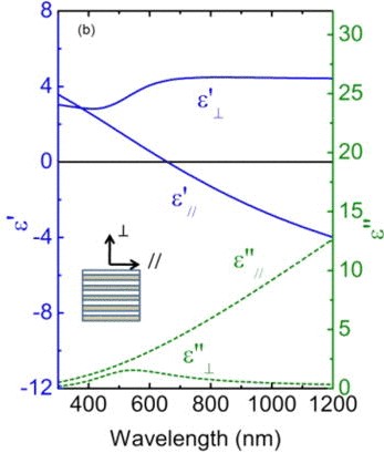 |
Light emitting silicon quantum dots by colloidal synthesis were uniformly spin-coated into a 20?nm-thick film and deposited atop a hyperbolic metamaterial of alternating TiN and SiO2 sub-wavelength layers. Using steady-state and time-resolved photoluminescence spectroscopy as a function of the emission wavelength in partnership with rigorous electromagnetic modeling of dipolar emission, we demonstrate enhanced Local Density of States and coupling to high-k modes in a broad spectral range. These findings provide an alternative approach for the engineering of novel Si-compatible broadband sources that leverage the control of radiative transitions in hyperbolic metamaterials and the flexibility of the widespread Si platform. |
| 212. Kenji Imakita, Takeshi Kamada, Jun-ichi Kamatani, Minoru Mizuhata,
and Minoru Fujii "Room Temperature Direct Imprinting of Porous Glass Prepared from Phase-Separated Glass", Nanotechnology, Vol. 26, 255304, pp. 1-8 (2015). (Published 5 June 2015) |
|
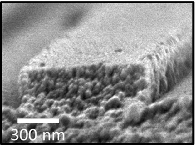 |
This work describes a room-temperature imprinting of nanoporous glass prepared by selective chemical etching of phase-separated glass. A highly porous (58%) and highly transparent (>90%) porous glass layer can be formed on a transparent phase-separated glass substrate. It is shown that the lateral resolution of the imprinting is a few tens of nanometers. As the porosity increases, the imprint depth increases and reaches up to 90% of the height of the mold pattern. The porous glass has a wider transmittance window (300?2700 nm) and a higher thermal durability (~500 °C) than other materials used for imprinting. The technique has various potential applications such as diffraction optical elements, waveguides, biosensors, and microfluidic devices. |
| 211. Toshihiro Nakamura, Sadao Adachi, Minoru Fujii, Hiroshi Sugimoto,
Kenta Miura and Shunya Yamamoto "Size and Dopant-Concentration Dependence of Photoluminescence Properties of Ion-Implanted Phosphorus- and Boron-Codoped Si Nanocrystals", Physical Review B, Vol. 91, 165424, pp. 1-8 (2015). (Published 22 April 2015) |
|
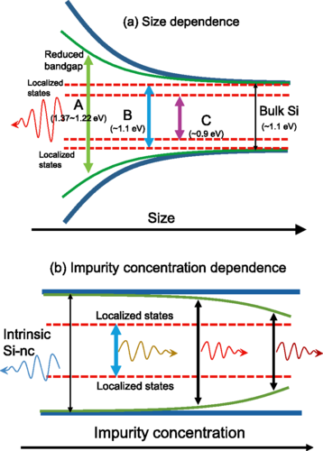 |
We investigate the nanocrystallite-size and dopant-concentration dependence of the photoluminescence (PL) properties of heavily phosphorus- (P) and boron- (B) codoped Si nanocrystals (Si NCs), prepared using a combination of sputtering and ion implantation techniques. We find that the heavily doped Si NC exhibits three exotic luminescence bands, A, B, and C. The peak energy of band A redshifts with increasing dopant concentration. This band is due to the band-to-band transition at the reduced Si-NC band gap caused by the formation of impurity bands together with band-tailing effects. The PL redshift becomes large when the nanocrystallite size decreases, suggesting the occurrence of the quantum-confinement-induced carrier doping effect. The peak energies of bands B and C are independent of both the concentration and size, indicating that these bands are due to transitions between defect- and/or impurity-related localized states. Band A shows stronger thermal quenching than the PL band in pure (undoped) Si NCs, the magnitude of which depends on the dopant concentration. The stronger thermal quenching in band A is probably due to the thermally induced migration of electrons in the impurity band. |
| 210. Ramesh Ghosh, P. K. Giri, Kenji Imakita and Minoru Fujii, "Photoluminescence Signature of Resonant Energy Transfer in ZnO Coated Si Nanocrystals Decorated On Vertical Si Nanowires Array", Journal of Alloys and Compounds, Vol. 638, pp. 419-428 (2015). (Final version published online: 31-MAR-2015) |
|
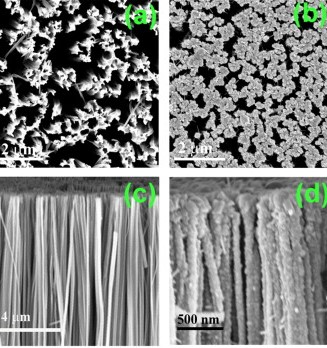 |
We investigate the mechanism of red shift in photoluminescence (PL) and reduction in the PL lifetime from Si nanocrystals (NCs) decorated on vertical Si nanowires (NWs) array due to ZnO over layer coating. Arrays of vertically aligned single crystalline Si NWs decorated with arbitrary shaped Si NCs have been fabricated by a silver assisted wet chemical etching method. A strong broad band and tunable visible to near-infrared PL is observed from these Si NWs at room temperature and the Si NCs on the surface of the Si NWs are primarily responsible for the PL emission. Higher band gap ZnO film is sputter deposited on the Si NCs decorated Si NWs to form heterostructure. Bare Si NW/NCs and Si NCs/ZnO heterostructures show extremely high broad band absorption in the entire visible region. PL studies on the Si NCs/ZnO heterostructures reveal significant red shift and in some cases reduced intensity of the PL band due to the ZnO layer in close proximity of the Si NCs. This is accompanied by a reduction in the PL lifetime of the Si NCs after ZnO coating. Interestingly, no measurable red shift in PL is observed in absence of the resonance in the visible PL emission energy of ZnO and that of Si NCs. The modified PL from the heterostructures is explained through an energy band diagram on the basis of resonant energy transfer from the defect assisted recombination of the carries in the ZnO overlayer that excites the Si NCs in the close proximity and subsequent de-excitation process via radiative recombination. These findings have important bearing on the development of cost effective Si-based hybrid optoelectronic devices using wide band gap heterostructured oxide semiconductors. |
| 209.Hiroshi Sugimoto, Minoru Fujii and Kenji Imakita, "Size-Controlled Growth of Cubic Boron Phosphide Nanocrystals", RSC Advances, Vol. 5, Issue 11, pp. 8427-8431 (2015). (First published online 24 Dec 2014) |
|
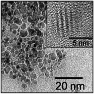 |
We report a new synthetic route for cubic boron phosphide (BP) nanocrystals with diameters of 2 to 6 nm. The key concept of the synthesis process is reduction of oxides of B and P in silicon (Si)-rich borophosphosilicate glass (BPSG) into cubic BP crystals by excess Si. The size of the cubic BP crystals is controlled by the composition of the starting materials. Free-standing cubic BP nanocrystals are extracted into solution by etching out BPSG matrices. The successful growth of size controlled cubic BP nanocrystals opens the way for the development of cubic BP nanocrystal-based optoelectronic and thermoelectric devices. |
| 208. Kaoru Yamamoto, Minoru Fujii, Shunji Sowa, Kenji Imakita, and Kanna
Aoki, "Upconversion Luminescence of Rare-Earth Doped Y2O3 Nanoparticle with Metal Nano-Cap", The Journal of Physical Chemistry C, Vol. 119, Issue 2, pp. 1175-1179 (2015). (Publication Date (Web): 19 Dec. 2014) |
|
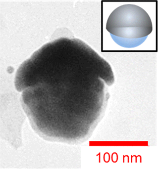 |
The upconversion property of an individual composite nanoparticle consisting of a metal (Ag) nanocap and a rare-earth doped upconversion nanoparticle (Er- and Yb-doped Y2O3 nanoparticle) was studied. The structural parameters of the composite nanoparticle were chosen so that the resonant wavelengths of the electric dipole and magnetic dipole surface plasmon modes of a nanocap coincide with the upconversion luminescence peaks of Er3+. Strong modification of the upconversion spectrum was observed by the formation of a Ag nanocap. Upon excitation at 980 nm, the green (?550 nm) and red (?670 nm) peaks were on average 23 and 48-fold, respectively, enhanced. The strong modification of the spectral shape, i.e., the intensity ratio of the green to red luminescence, suggests that the enhancement of radiative decay rates by the two surface plasmon modes is mainly responsible for the upconversion enhancement. |
| 207. Hui Lin, Kenji Imakita, and Minoru Fujii, "Reversible Emission Evolution from Ag Activated Zeolite Na-A upon Dehydration/Hydration", Applied Physics Letters, Vol. 105, 211903, pp. 1-4 (2014). (Publication Date (Web):25 Nov. 2014) (Copyright (2014) American Institute of Physics. This article may be downloaded for personal use only. Any other use requires prior permission of the author and the American Institute of Physics. ) |
|
 |
Reversible emission evolution of thermally treated Ag activated zeolite Na-A upon dehydration/hydration in vacuum/water vapor was observed. The phenomenon was observed even for the sample with low Ag+-Na+ exchanging (8.3%), indicating that the emission from Ag activated zeolites may not come from Ag clusters while from the surrounding coordinated Ag+ ions or Ag0 atoms. It was disclosed that the characteristic yellow-green emission at ?560?±?15?nm is strongly associated with the coordinating water molecules to the Ag+ ions or Ag0 atoms, which is clear evidence for that the efficient emission from Ag activated zeolites may not originate from the quantum confinement effect. |
| 206. Zhenhua Bai, Hui Lin, Kenji Imakita, Reza Montazami, Minoru Fujii
and Nastaran Hashemi, "Synthesis of Er3+/Yb3+ Codoped NaMnF3 Nanocubes with Single-Band Red Upconversion Luminescence", RSC Advances, Vol. 4, Issue 106, pp. 61891-61897 (2014). (Publication Date (Web): 11 Nov. 2014) |
|
 |
We have developed a facile low-temperature synthetic method for the preparation of NaMnF3 nanocubes with Er3+ and Yb3+ ions homogeneously incorporated in the host lattice. The effects of the reaction temperature, and the volume ratio between ethanol and DI water on the morphology of NaMnF3 nanocubes are systematically investigated. The NaMnF3 nanocubes can be produced in the low temperature range (25?80 °C), and the higher reaction temperature (80 °C) is favorable for the formation of a smooth surface. The formation of NaMnF3 nanocubes strongly depends on the ethanol solvent. The morphology and single-phase of the obtained samples could be well maintained by controlling the doping concentration (Yb3+ ? 20 mol%). Single-band red upconversion emission can be generated in Er3+/Yb3+ codoped NaMnF3 nanocubes due to the energy transfer between host Mn2+ and dopant Er3+ ions. It is revealed that our NaMnF3:Er3+/Yb3+ nanocubes irradiate the brightest red luminescence at the dopant concentrations of Er3+ (2 mol%) and Yb3+ (15 mol%), which is stronger than that of the hexagonal-phase NaYF4:Er3+/Yb3+ phosphor. |
| 205. Sa Chu Rong Gui, Kenji Imakita, Hui Lin, and Minoru Fujii, "Ag and Dy Doped Zeolite as a Broadband Phosphor", Optical Materials, Vol. 38, Issue , pp. 75-79 (2014). (Publication Date (Web): 2014) |
|
 |
Photoluminescence (PL) properties of silver (Ag) and dysprosium (Dy) codoped zeolites were investigated. It was found that PL from the 4F9/2?6H13/2 transition of Dy3+ ions at 575 nm is more than 50 times enhanced by the presence of Ag+ ions under ultraviolet excitation. The excitation wavelength dependence of the PL intensity coincided well with the absorption spectra of Ag+ ions, indicating that Dy3+ ions are excited by the energy transfer from Ag+ ions. In addition, by carefully optimizing annealing condition and Dy and Ag concentration, white light was realized due to the combination of blue emission of Ag+ ions, yellow emission of Dy3+ ions and red emission of Ag clusters. |
| 204. Ibuki Kawamura, Kenji Imakita, Akihiro Kitao, and Minoru Fujii, "Polarization-Sensitive Second Harmonic Generation Microscopy of α-quartz like GeO2 (α-GeO2) Polycrystal", Journal of Physics D: Applied Physics, Vol. 47, 455305, pp. 1-7 (2014). (Publication Date (Web): 2014) |
|
 |
The usefulness of polarized second harmonic generation (SHG) microscopy to determine crystallographic orientations of domains in polycrystalline films was demonstrated. Orientation of α-quartz like GeO2 (α-GeO2) domains in polycrystalline films were investigated by using polarized SHG and Raman microscopy. It was found that the SHG intensity of a α-GeO2 polycrystalline film depends strongly on measurement points and excitation and detection polarizations, while the Raman intensity was almost uniform in the whole mapping area. Analyses of the SHG mappings in different polarization conditions allowed us to determine not only the size and shape of crystalline domains, but also the crystallographic orientations. |
| 203. Hiroshi Sugimoto, Minoru Fujii, and Kenji Imakita, "Synthesis of Boron and Phosphorus Codoped All-Inorganic Colloidal Silicon Nanocrystals from Hydrogen Silsesquioxane", Nanoscale, Vol. 6, Issue 21, pp. 12354-12359 (2014). (Publication Date (Web): 21 Aug 2014) |
|
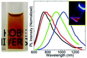 |
We present a new route for mass-production of B and P codoped all-inorganic colloidal Si nanocrystals (NCs) from hydrogen silsesquioxane (HSQ). Codoped Si NCs are grown in glass matrices by annealing mixture solutions of HSQ and dopant acids, and then extracted from the matrices by hydrofluoric acid etching. The free-standing NCs are dispersible in methanol without any surface functionalization processes. The structural analyses suggest the formation of heavily B and P doped hydrophilic shells on the surface of Si NCs. The NCs show efficient size-tunable photoluminescence in the near infrared to visible region. |
| 202. Hiroki Shibata, Kenji Imakita, and Minoru Fujii, "Fabrication of a Core-Shell-Shell Particle with a Quarter-Wave Thick Shells and Its Optical Properties", RSC Advances, Vol. 4, Issue 61, pp. 32293-32297 (2014). (Publication Date (Web): July 14, 2014) |
|
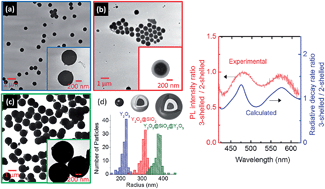 |
A multi-shelled sphere with a quarter-wave thick shell is known to act as a spherical Bragg resonator with a complete photonic band gap and have potential applications in photonics. However, no fabrication techniques have been established. In this work, core?shell?shell particles with quarter-wave thick shells were synthesized by chemical solution processes for the first time. They consist of a Ce3+ doped Y2O3 nanoparticle core, a SiO2 first shell, and a Y2O3 second shell. The core and the second shell were fabricated by a homogeneous precipitation method and the first shell by a sol?gel method. By carefully optimizing the reaction conditions, the shell thickness was controlled to a quarter optical wavelength for visible (500 nm) light with the standard deviation of thickness of the order of several nanometers. The scattering and photoluminescence spectra of single particles were studied, and they were well reproduced by Mie theory. The results indicate that the luminescence properties of the nanoparticles can be modified by the quarter-wave thick shells. The procedures can be extended for the fabrication of multi-shelled photonic bandgap structures, by simply repeating the SiO2 and Y2O3 coating processes. |
| 201. Hui Lin, Kenji Imakita, Sa Chu Rong Gui, and Minoru Fujii, "Near Infrared Emission from Molecule-Like Silver Clusters Confined in Zeolite A Assisted by Thermal Activation", Journal of Applied Physics, Vol. 116, Issue 3, 013509, pp. 1-5 (2014). (Publication Date (Web): July 03, 2014) (Copyright (2014) American Institute of Physics. This article may be downloaded for personal use only. Any other use requires prior permission of the author and the American Institute of Physics. ) |
|
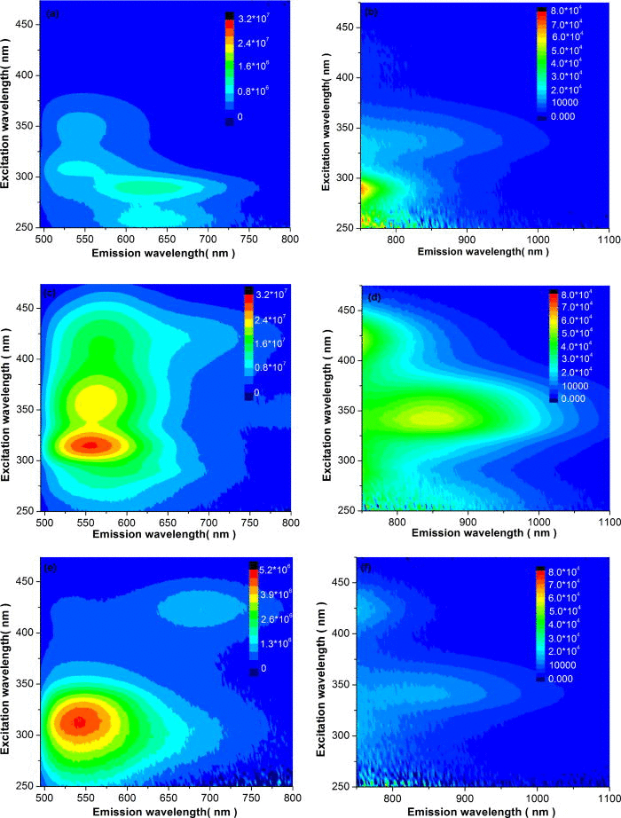 |
Strong and broad near infrared (NIR) emission peaked at ?855?nm upon optimal excitation at 342?nm has been observed from molecule-like silver clusters (MLSCs) confined in zeolite A assisted by thermal activation. To the best of our knowledge, this is the first observation of NIR emission peaked at longer than 800?nm from MLSCs confined in solid matrices. The decay time of the NIR emission is over 10 μs, which indicates that it is a spin-forbidden transition. The ?855?nm NIR emission shows strong dependence on the silver loading concentration and the thermal activation temperature. |
| 200. Soumen Dhara, Kenji Imakita, P Giri, and Minoru Fujii, "Strain Dependence of the Nonlinear Optical Properties of Strained Si Nanoparticles", Optics Letters, Vol. 39, Issue 13, pp. 3833-3836 (2014). (Publication Date (Web): May 27, 2014) |
|
 |
We report on the lattice strain dependence of the nonlinear optical (NLO) parameters of strained Si nanoparticles (NPs), which are prepared in a controlled way by a mechanical ball milling process. X-ray diffraction analysis shows that the nature of strain is compressive and is primarily caused by milling-induced lattice dislocations, which is further supported by high-resolution transmission electron microscopy imaging. It is found that the nonlinear refractive index ( 2) and nonlinear absorption coefficient ( ) are strongly influenced by the associated lattice strain present in Si NPs. With the increase of lattice strain, the gradually decreases while 2 increases slowly. The strain-dependent observed changes in the NLO parameters of Si NPs are found to be advantageous for application purpose, and it is explained on the basis of strain-induced modification in the electronic structure of the highest occupied molecular orbital and lowest unoccupied molecular orbital states of Si NPs. These results demonstrate the potential of strain-dependent enhancement of nonlinearities for silicon photonics applications. |
| 199. Takashi Kanno, Minoru Fujii, Hiroshi Sugimoto, and Kenji Imakita, "Colloidal Silicon Germanium Alloy Nanocrystals with High Boron and Phosphorus Concentration Hydrophilic Shell", The Journal of Materials Chemistry C, Vol. 2, Issue 28, pp. 5644-5650 (2014). (Publication Date (Web):25 Apr 2014) |
|
 |
Si1?xGex alloy nanocrystals potentially have superior properties compared to Si nanocrystals such as an enhanced absorption cross-section and wider controllability of the band gap energy. However, reports on the synthesis of Si1?xGex alloy nanocrystals, especially colloidal Si1?xGex alloy nanocrystals, are still very limited and the quality is not as high as that of colloidal Si nanocrystals. Here, we report the development of a new type of luminescent colloidal Si1?xGex alloy nanocrystals of 3 to 6 nm in diameter. The characteristic feature of the Si1?xGex alloy nanocrystals is the formation of a high B and P concentration layer on the surface. The shell provides inorganic atomic ligands and B and P co-doped Si1?xGex nanocrystals can be dispersed in alcohol without any surface functionalization processes. |
| 198. Batakrushna Santara, Parvat Giri, Soumen Dhara, Kenji Imakita, and
Minoru Fujii, "Oxygen Vacancy Mediated Enhanced Ferromagnetism in Undoped and Fe Doped TiO2 Nanoribbons", Journal of Physics D: Applied Physics, Vol. 47, 235304, pp. 1-14 (2014). (Publication Date (Web):) |
|
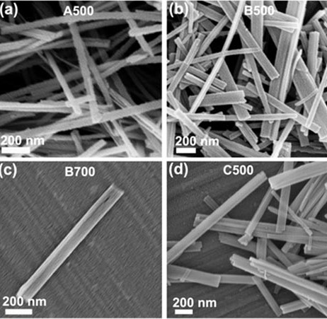 |
We have investigated the structural, optical and ferromagnetic properties of undoped and Fe-doped TiO2 nanoribbons (NRbs) grown by a solvothermal method. A strong room temperature ferromagnetism (RTFM) is observed in both undoped and Fe-doped TiO2 NRbs. Fe-doped TiO2 NRbs exhibited a ~4.8-fold enhancement in RTFM as compared to the undoped NRbs grown under similar conditions. However, the RTFM decreases at higher Fe concentration, possibly due to antiferromagnetic ordering between nearby Fe3+ ions caused by a super exchange interaction. X-ray diffraction patterns reveal the pure TiO2(B) phase, the TiO2(B)?anatase mixed phase and the anatase?rutile mixed phase of the TiO2 structure. Field emission scanning electron microscopy and transmission electron microscopy observations reveal NRbs with uniform pore distribution and nanopits formed on the surface for both undoped and Fe-doped NRbs. These samples exhibit strong visible photoluminescence associated with oxygen vacancies and the ferromagnetic hysteresis loop, both of which are strongly enhanced after vacuum annealing. Optical absorption, electron spin resonance and x-ray photoelectron spectroscopic analyses are performed to elucidate the origin of RTFM. The observed RTFM in undoped and Fe-doped TiO2 NRbs is qualitatively explained through a model involving bound magnetic polarons, which include an electron locally trapped by an oxygen vacancy with the trapped electron occupying an orbital overlapping with the unpaired electron (3d1) of a Ti3+ ion and/or the unpaired electron (3d5) of a Fe3+ ion. The development of TiO2 NRbs with tunable optical and magnetic properties constitutes an important step towards realizing improved magneto-optical and spintronic devices from novel TiO2 nanostructures. |
| 197. Akihiro Kitao, Kenji Imakita, Ibuki Kawamura, and Minoru Fujii, "Investigation of Second Harmonic Generation from Si Rich SiNx Thin Films Deposited by rf Sputtering over a Wide Range of Si Concentration", Journal of Physics D, Vol. 47, 215101, pp. 1-8 (2014). (Publication Date (Web):) |
|
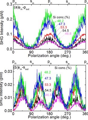 |
The second-order nonlinearity of Si-rich SiNx thin films prepared by RF sputtering was investigated. It was found that the second-order nonlinear coefficient (deff) increases with increasing Si concentration in a wide range of Si concentrations. The observed maximum value of deff was 5.9 pm V?1, which is twice that of the β-BaB2O4 crystal. X-ray photoelectron spectroscopy analysis in the Si 2p energy region revealed that the films consist of Si species with different valence states. Strong correlation was observed between the deff values and the XPS peak intensity of Si0 species, suggesting that Si clusters are the most probable origin of the large second-order nonlinearity. |
| 196. Soumen Dhara, Kenji Imakita, Minoru Mizuhata, and Minoru Fujii, "Europium Doping Induced Symmetry Deviation and its Impact on the Second Harmonic Generation of Doped ZnO Nanowires", Nanotechnology, Vol. 25, No. 22, 225202, pp. 1-10 (2014). (Publication Date (Web):) |
|
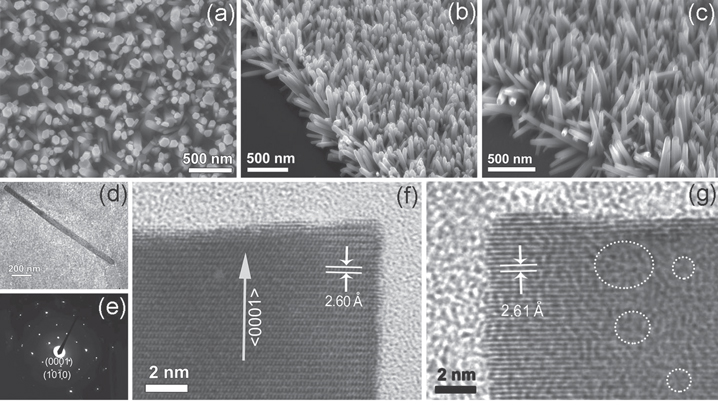 |
In this work, we investigated the effects of europium doping on the second harmonic generation (SHG) of ZnO nanowires (NWs). A non-monotonic enhancement in the SHG is observed with the increase of the europium concentration. Maximum SHG is observed from the 1 at.% europium doped ZnO NWs with an enhancement factor of 4.5. To understand the underlying mechanism, the effective second order non?linear coefficient (deff) is calculated from the theoretical fitting with consideration of the absorption effect. Microstructural characterization reveals the structural deformation of the ZnO NWs caused by europium doping. We estimated the deviation in the crystal site symmetry around the Eu3+ ions (defined as the asymmetric factor) from photoluminescence measurement and it is found to be strongly correlated with the calculated deff value. A strong linear dependence between the magnitudes of deff and the asymmetric factor suggests that deviation in the local site symmetry of the ZnO crystal by europium doping could be the most probable origin of the observed large second order non-linearity. |
| 195. Batakrushn Santara, Parvat Giri, Kenji Imakita, and Minoru Fujii, "Microscopic Origin of Lattice Contraction and Expansion in Undoped Rutile TiO2 Nanostructures", Journal of Physics D, Vol. 47, 215302, pp. 1-13 (2014). (Publication Date (Web): 25 March 2014) |
|
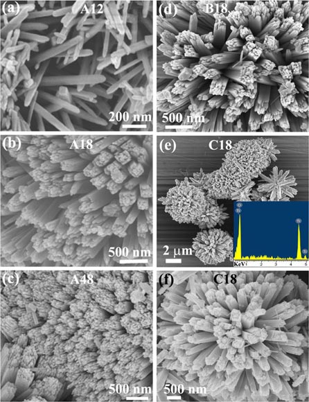 |
We have investigated the microscopic origin of lattice expansion and contraction in undoped rutile TiO2 nanostructures by employing several structural and optical spectroscopic tools. Rutile TiO2 nanostructures with morphologies such as nanorods, nanopillars and nanoflowers, depending upon the growth conditions, are synthesized by an acid-hydrothermal process. Depending on the growth conditions and post-growth annealing, lattice contraction and expansion are observed in the nanostructures and it is found to correlate with the nature and density of intrinsic defects in rutile TiO2. The change in lattice volume correlates well with the optical bandgap energy. Irrespective of growth conditions, theTiO2 nanostructures exhibit strong near infrared (NIR) photoluminescence (PL) at 1.43 eV and a weak visible PL, which are attributed to the Ti interstitials and O vacancies, respectively, in rutile TiO2 nanostructures. Further, ESR study reveals the presence of singly ionized oxygen vacancy defects. It is observed that lattice distortion depends systematically on the relative concentration and type of defects such as oxygen vacancies and Ti interstitials. XPS analyses revealed a downshift in energy for both Ti 2p and O 1s core level spectra for various growth conditions, which is believed to arise from the lattice distortions. It is proposed that the Ti4+ interstitial and F+ oxygen vacancy defects are primarily responsible for lattice expansion, whereas the electrostatic attraction between Ti4+ interstitial and O2? interstitial defects causes the lattice contraction in the undoped TiO2 nanostructures. The control of lattice parameters through the intrinsic defects may provide new routes to achieving novel functionalities in advanced materials that can be tailored for future technological applications. |
| 194. Minoru Fujii, Hiroshi Sugimoto, Masataka Hasegawa, and Kenji Imakita, "Silicon Nanocrystals with High Boron and Phosphorus Concentration Hydrophilic Shell -Raman Scattering and X-Ray Photoelectron Spectroscopic Studies", Journal of Applied Physics, Vol. 115, Issue 8, 084301, pp. 1-5 (2014). (Publication Date (Web):24 February 2014) (Copyright (2014) American Institute of Physics. This article may be downloaded for personal use only. Any other use requires prior permission of the author and the American Institute of Physics. ) |
|
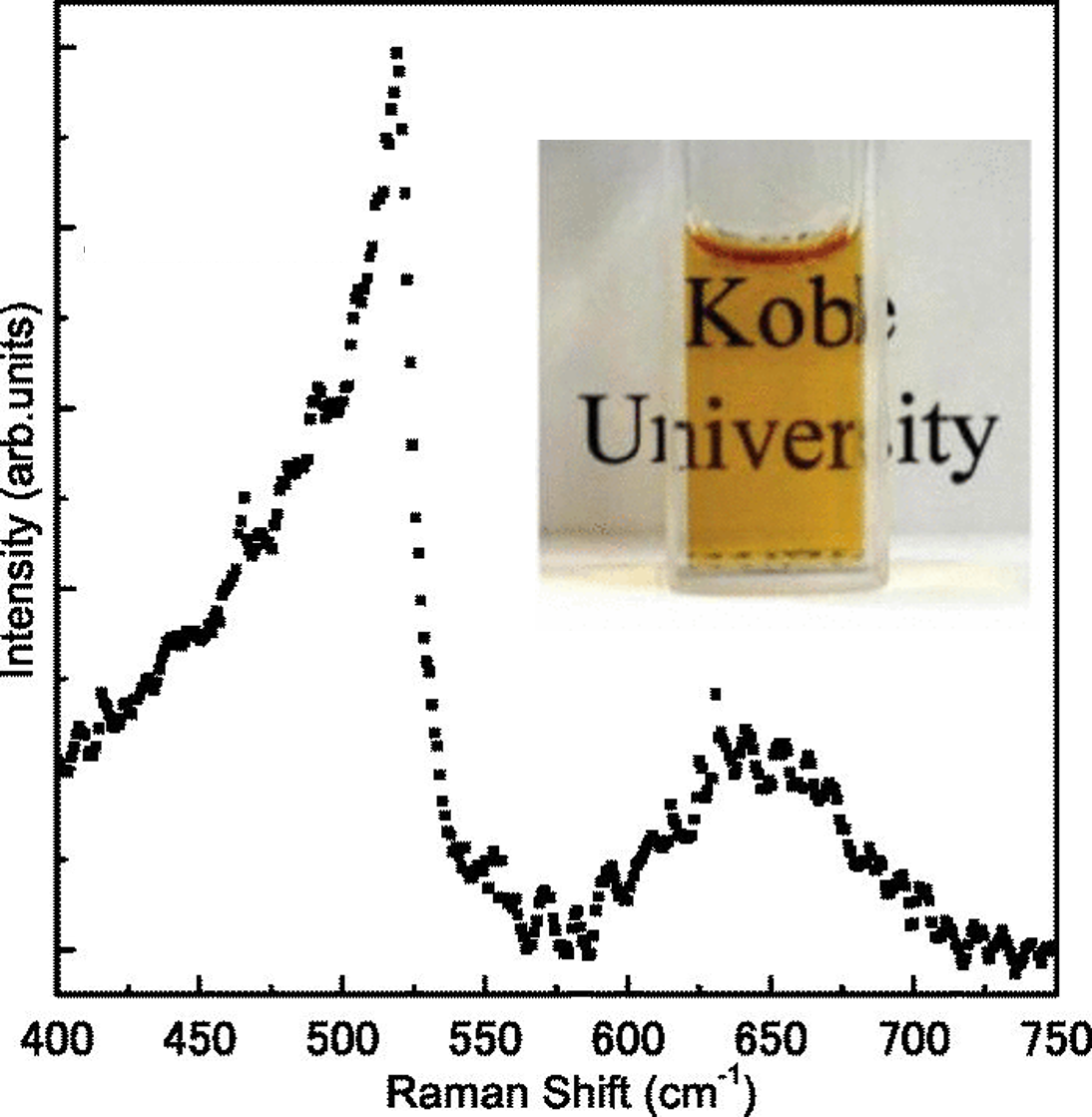 |
Boron (B) and phosphorus (P) codoped silicon (Si) nanocrystals, which exhibit very wide range tunable luminescence due to the donor to acceptor transitions and can be dispersed in polar liquids without organic ligands, are studied by Raman scattering and X-ray photoelectron spectroscopies. Codoped Si nanocrystals exhibit a Raman spectrum significantly different from those of intrinsic ones. First, the Raman peak energy is almost insensitive to the size and is very close to that of bulk Si crystal in the diameter range of 2.7 to 14?nm. Second, the peak is much broader than that of intrinsic ones. Furthermore, an additional broad peak, the intensity of which is about 20% of the main peak, appears around 650?cm?1. The peak can be assigned to local vibrational modes of substitutional B and B-P pairs, B clusters, B-interstitial clusters, etc. in Si crystal. The Raman and X-ray photoelectron spectroscopic studies suggest that a crystalline shell heavily doped with these species is formed at the surface of a codoped Si nanocrystal and it induces the specific properties, i.e., hydrophilicity, high-stability in water, high resistance to hydrofluoric acid, etc. |
| 193. Hui Lin, Sa Chu Rong Gui, Kenji Imakita, and Minoru Fujii, "Enhanced NIR Emission from the Partially Vitrified Nd3+ and Silver Co-doped Zeolite Y", Journal of Applied Physics, Vol. 115, 033507, pp. 1-7 (2014). (Publication Date (Web): January 16, 2014) |
|
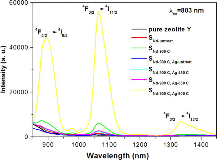 |
Near infrared (NIR) emission from the Nd3+ doped zeolite Y was strongly enhanced by partially vitrifying the zeolite structure via extra loading silver ions and post annealing. Under the low annealing temperatures at 450?°C and 650?°C, the states of the loaded silver were determined to be the co-existence of the isolated Ag0 atoms, the Ag+ ions, and the Ag2+ dimers. However, there was no enhancement in the NIR emission by the introduction of these small silver clusters. Under higher annealing temperature at 900?°C where the lattice of the zeolite Y was partially collapsed into the amorphous phase, strong NIR emission enhancement at 1064?nm with a factor of 6.8 was observed. The partial vitrification process by the co-loading of silver and post heat-treatment had strong effect on eliminating the H2O molecules, which can greatly enhance the NIR emission. |
| 192. Ravi K. Biroju, P. K. Giri, Soumen Dhara, Kenji Imakita, and Minoru
Fujii, "Graphene-Assisted Controlled Growth of Highly Aligned ZnO Nanorods and Nanoribbons: Growth Mechanism and Photoluminescence Properties", ACS Applied Materials and Interfaces, Vol. 6, Issue. 1, pp. 377-387 (2014). (Publication Date (Web): December 16, 2013) |
|
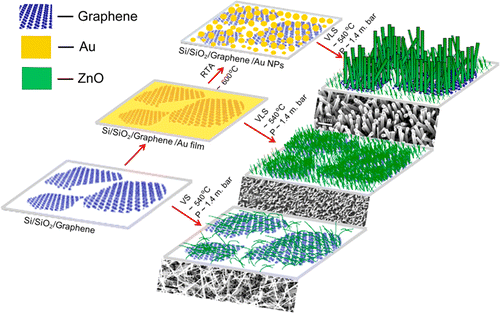 |
We demonstrate graphene-assisted controlled fabrication of various ZnO 1D nanostructures on the SiO2/graphene substrate at a low temperature (540 °C) and elucidate the growth mechanism. Monolayer and a few layer graphene prepared by chemical vapor deposition (CVD) and subsequently coated with a thin Au layer followed by rapid thermal annealing is shown to result in highly aligned wurtzite ZnO nanorods (NRs) with clear hexagonal facets. On the other hand, direct growth on CVD graphene without a Au catalyst layer resulted in a randomly oriented growth of dense ZnO nanoribbons (NRBs). The role of in-plane defects and preferential clustering of Au atoms on the defect sites of graphene on the growth of highly aligned ZnO NRs/nanowires (NWs) on graphene was established from micro-Raman and high-resolution transmission electron microscopy analyses. Further, we demonstrate strong UV and visible photoluminescence (PL) from the as-grown and post-growth annealed ZnO NRs, NWs, and NRBs, and the origin of the PL emission is correlated well with the X-ray photoelectron spectroscopy analysis. Our results hint toward an epitaxial growth of aligned ZnO NRs on graphene by a vapor?liquid?solid mechanism and establish the importance of defect engineering in graphene for controlled fabrication of graphene?semiconductor NW hybrids with improved optoelectronic functionalities. |
| 191.Sa chu rong gui, Kenji Imakita, Minoru Fujii, and Shinji Hayashi, "Photosensitization of Europium Ions by Silver Clusters in Zeolite", Optical Materials, Vol. 36, 5, pp. 916-920 (2014). (Publication Date (Web): December 21, 2013) |
|
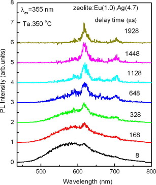 |
Photosensitization of europium (Eu) ions by silver (Ag) clusters was achieved by simultaneously doping Eu and Ag in zeolite cages. The photoluminescence (PL) due to the 5D0 → 7F2 transition of Eu ions at 613 nm is significantly increased by the presence of Ag clusters. The excitation wavelength dependence of the PL intensity coincided well with the absorption spectrum of Ag clusters, indicating that Eu ions are excited by the energy transfer from Ag clusters. |
| 190. Zhenhua Bai, Hui Lin, Jesse Johnson, Sa Chu Rong Gui, Kenji Imakita,
Reza Montazami, Minoru Fujii, and Nastaran Hashemi, "The Single-Band Red Upconversion Luminescence from Morphology and Size Controllable Er3+/Yb3+ doped MnF2 Nanostructures", Journal of Materials Chemistry C, Vol. 2, 9, pp.1736-1741 (2014). (Publication Date (Web): December 9, 2013) |
|
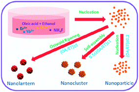 |
Er3+/Yb3+ doped MnF2 nanostructures have been prepared via a solvothermal method. The morphology of the nanocrystals could be well controlled from nanoparticles to nanoclusters and nanolanterns by varying the volume ratio between oleic acid and ethanol in the solvent. Moreover, the size is tuned from 200 nm to 1.5 μm with the increase of reaction temperature from 110 to 200 °C. It is shown that controlling the doping concentration (Yb3+ ? 20 mol%) is essential to preserve the single phase and morphology of the MnF2 host. Single-band red upconversion (UC) emission can be generated in Er3+ single and Er3+/Yb3+ codoped MnF2 nanoclusters due to the energy transfer between host Mn2+ and dopant Er3+ ions. The detailed studies suggest that our MnF2:Er3+/Yb3+ nanocrystals have the strongest single-band luminescence feature at the dopant concentrations of Er3+ (2 mol%) and Yb3+ (20 mol%). The brighter red emission from the current nanostructure compared with those from NaYF4:Er3+/Yb3+ has shown its suitability as an efficient UC luminescence host. It is expected that the achieved intense pure red emission may have potential application in in vivo bioimaging. |
| 189. Ramesh Ghosh, Parvat Giri, Kenji Imakita, and Minoru Fujii, "Origin of Visible and Near Infrared Photoluminescence from Chemically Etched Si Nanowires Decorated with Arbitrary Shaped Si Nanocrystals", Nanotechnology, Vol. 25, No. 4, 045703, pp. 1-13 (2014). (Publication Date (Web): November 26, 2013) |
|
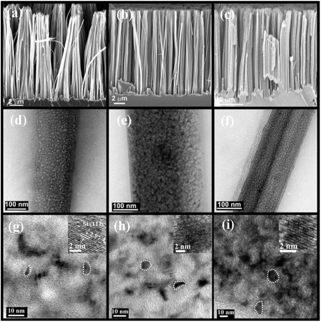 |
Arrays of vertically aligned single crystalline Si nanowires (NWs) decorated with arbitrarily shaped Si nanocrystals (NCs) have been fabricated by a silver assisted wet chemical etching method. Scanning electron microscopy and transmission electron microscopy are performed to measure the dimensions of the Si NWs as well as the Si NCs. A strong broad band and tunable visible (2.2 eV) to near-infrared (1.5 eV) photoluminescence (PL) is observed from these Si NWs at room temperature (RT). Our studies reveal that the Si NCs are primarily responsible for the 1.5?2.2 eV emission depending on the cross-sectional area of the Si NCs, while the large diameter Si/SiOx NWs yield distinct NIR PL consisting of peaks at 1.07, 1.10 and 1.12 eV. The latter NIR peaks are attributed to TO/LO phonon assisted radiative recombination of free carriers condensed in the electron?hole plasma in etched Si NWs observed at RT for the first time. Since the shape of the Si NCs is arbitrary, an analytical model is proposed to correlate the measured PL peak position with the cross-sectional area (A) of the Si NCs, and the bandgap (Eg) of nanostructured Si varies as Eg = Eg (bulk) + 3.58 A?0.52. Low temperature PL studies reveal the contribution of non-radiative defects in the evolution of PL spectra at different temperatures. The enhancement of PL intensity and red-shift of the PL peak at low temperatures are explained based on the interplay of radiative and non-radiative recombinations at the Si NCs and Si/SiOx interface. Time resolved PL studies reveal bi-exponential decay with size correlated lifetimes in the range of a few microseconds. Our results help to resolve a long standing debate on the origin of visible?NIR PL from Si NWs and allow quantitative analysis of PL from arbitrarily shaped Si NCs. |
| 188. Sa chu rong gui, Kenji Imakita, Minoru Fujii, and Shinji Hayashi, "Enhanced Red Photoluminescence of Samarium in Zeolite A by Interaction with Silver Ions", Japanese Journal of Applied Physics, Vol. 43, 022102, pp. 1-4 (2014). (Publication Date (Web): November 25, 2013) |
|
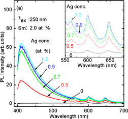 |
Photosensitization of samarium (Sm) ions by silver (Ag) ions was achieved by simultaneously doping Sm and Ag in zeolite A cages. Photoluminescence (PL) from the 4G2/5 → 6H2/7 transition of Sm ions at 600 nm was found to be more than 30 times enhanced by the presence of Ag ions. The excitation wavelength dependence of the PL intensity coincided well with the absorption spectra of Ag ions in the ultraviolet region, indicating that Sm ions are excited by the energy transfer from Ag ions. |
| 187. Hiroshi Sugimoto, Minoru Fujii, Yuki Fukuda, Kenji Imakita and Kensuke
Akamatsu , "All-Inorganic Water-Dispersible Silicon Quantum Dots: Highly Efficient Near-Infrared Luminescence in a Wide pH Range", Nanoscale, Vol. 6, Issue 1, pp. 122-126 (2014). (Accepted 08 Oct 2013, First published online 10 Oct 2013) |
|
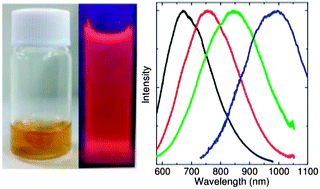 |
We report a novel method to prepare silicon quantum dots (Si-QDs) having excellent stability in water without organic-ligands by simultaneously doping phosphorus and boron. The codoped Si-QDs in water exhibit bright size-tunable luminescence in a biological window. The luminescence of codoped Si-QDs is very stable under continuous photoexcitation in water. |
| 186. Zhenhua Bai, Minoru Fujii, Kenji Imakita, and Shinji Hayashi, "Strong White Photoluminescence from Annealed Zeolites", Journal of Luminescence, Vol. 145, pp. 288-291 (2014). (Accepted 2 August 2013 Available online 12 August 2013) |
|
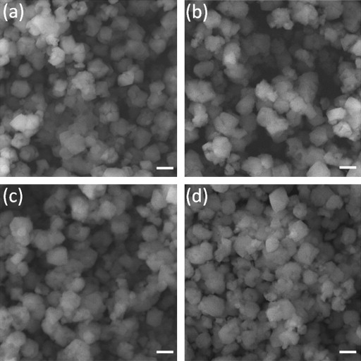 |
The optical properties of zeolites annealed at various temperatures are investigated for the first time. The annealed zeolites exhibit strong white photoluminescence (PL) under ultraviolet light excitation. With increasing annealing temperature, the emission intensity of annealed zeolites first increases and then decreases. At the same time, the PL peak red-shifts from 495 nm to 530 nm, and then returns to 500 nm. The strongest emission appears when the annealing temperature is 500 °C. The quantum yield of the sample is measured to be ~10%. The PL lifetime monotonously increases from 223 μs to 251 μs with increasing annealing temperature. The origin of white PL is ascribed to oxygen vacancies formed during the annealing process. |
| 185. Ibuki Kawamura, Kenji Imakita, Minoru Fujii, and Shinji Hayashi "Second Harmonic Generation from Ge Doped SiO2 (Gex(SiO2)1-x) Thin Films Grown by Sputtering", Applied Physics Letters, Vol. 103, Issue 20, 201117, pp. 1-3 (2013). |
|
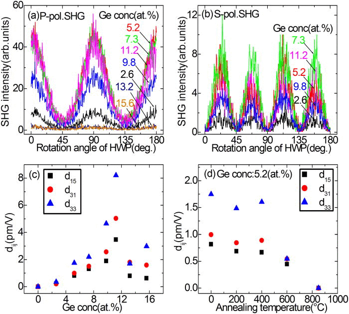 |
Second-order nonlinear optical properties of sputter-deposited Ge-doped SiO2 thin films were investigated. It was shown that the second-order nonlinearity of SiO2, which vanishes in the electric-dipole approximation due to the centrosymmetric structure, can be significantly enhanced by Ge doping. The observed maximum value of d33 was 8.2?pm/V, which is 4 times larger than d22 of β-BaB2O4 crystal. Strong correlation was observed between the deff values and the electron spin resonance signals arising from GePb centers, suggesting that GePb centers are the most probable origin of the large second-order nonlinearity. |
| 184. Kenji Imakita, Takeshi Kamada, Minoru Fujii, Kanna Aoki, Minoru Mizuhata,
and Shinji Hayashi "A Terahertz Wire Grid Polarizer Fabricated by Imprinting Porous Silicon", Optics Letters, Vol. 38, Issue 23, pp. 5067-5070 (2013). |
|
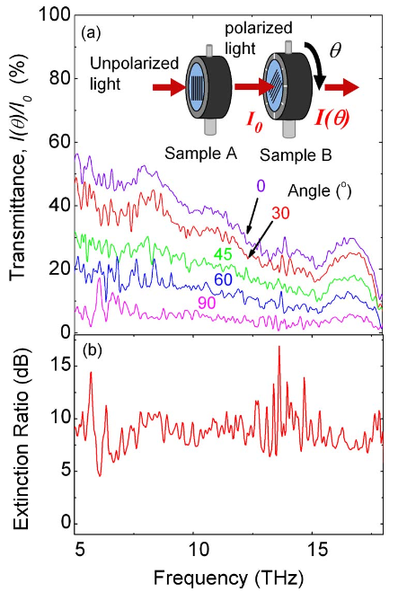 |
A terahertz (THz) wire-grid polarizer is fabricated by imprinting porous Si followed by oblique evaporation of Ag. We demonstrate that it works in a wide frequency region covering from 5 to 18 THz with the extinction ratio of 10 dB. The frequency region is much wider than that of THz wire-grid polarizers fabricated by conventional imprint lithography using organic materials. The result suggests that imprinting of porous Si is a promising fabrication technique to realize low-cost wire-grid polarizers working in the THz region. |
| 183. Batakrushna Santara , Pravat Kumar Giri , Kenji Imakita , and Minoru
Fujii, "Evidence for Ti Interstitial Induced Extended Visible Absorption and Near Infrared Photoluminescence from Undoped TiO2 Nanoribbons: An In-Situ Photoluminescence Study", The Journal of Physical Chemistry C, Vol. 117, Issue 44, pp. 23402-23411 (2013). |
|
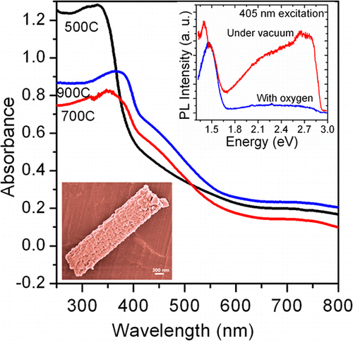 |
Despite decades of research on the role of intrinsic defects in enhancing the performance of reduced TiO2 based materials, unambiguous identification of defects responsible for visible light absorption, and near-infrared (NIR) photoluminescence from undoped TiO2 has remained challenging. Herein, through in situ photoluminescence (PL) studies under a controlled environment, we investigated the origin of an extended visible absorption, visible and NIR PL emission from undoped TiO2 nanoribbons grown by a solvothermal route. Our studies reveal that oxygen vacancies, Ti3+, and F+ center in TiO2 are responsible for absorption in the violet and blue-green region and the PL emission in the visible region. On the other hand, absorption in the yellow-red to NIR region and PL emission in the NIR region at 1.47 and ?1.30 eV are due to Ti4+ and Ti3+ interstitials, respectively, near the surface identified for the first time. The above conclusions are supported by electron paramagnetic resonance and X-ray photoelectron spectroscopy analyses. The development of such nanoporous undoped TiO2 nanoribbons with strong visible absorption and optical identification of Ti interstitial induced band gap states serves as an important milestone toward realizing improved visible light photocatalytic and photovoltaic applications of this novel material. |
| 182. Soumen Dhara, Kenji Imakita, P. K. Giri1, Minoru Mizuhata, and Minoru
Fujii, "Aluminum Doped Core-Shell ZnO/ZnS Nanowires: Doping and Shell Layer Induced Modification on Structural and Photoluminescence Properties", Journal of Applied Physics, Vol. 114, Issue 13, 134307 (2013), pp. 1-8 (2013). (Copyright (2013) American Institute of Physics. This article may be downloaded for personal use only. Any other use requires prior permission of the author and the American Institute of Physics. ) |
|
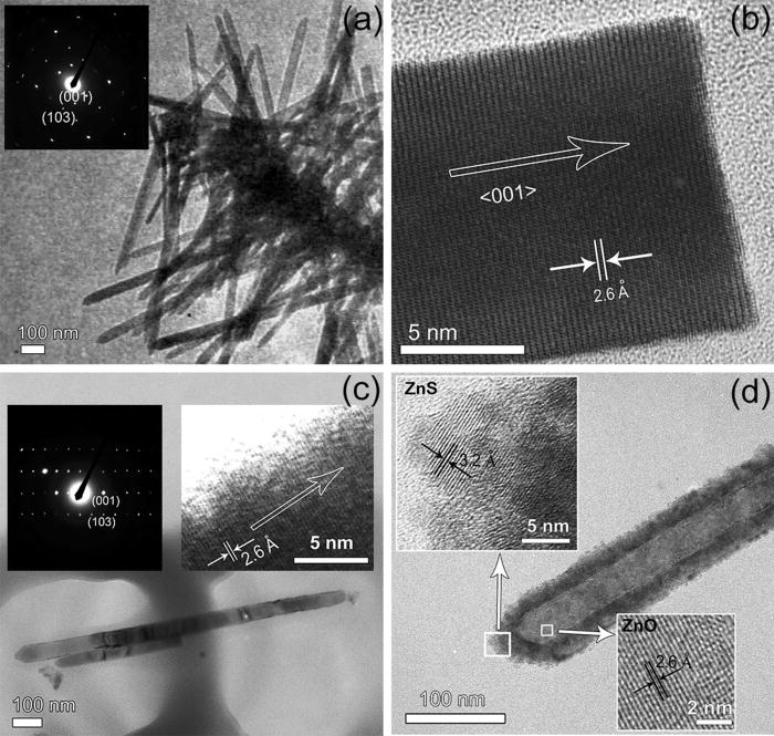 |
In this work, we investigated the combined effects of Al doping and surface modification on the fabrication of a core?shell type ZnO/ZnS nanowires (NWs) and its structural, electrical, and photoluminescence (PL) properties. A systematic investigation for different concentrations of Al doping followed by surface modification with different thicknesses of ZnS layer was performed. Significant changes in the nature of PL spectra and electronic conductivity are observed and insight discussions are present. Structural characterization on the core-shell NWs reveals the successful fabrication of Al doped highly single crystalline ZnO core and polycrystalline ZnS shell with both ZnO and ZnS are of hexagonal wurtzite structure. Compared with the bare undoped ZnO NWs, Al doped core-shell ZnO/ZnS NWs exhibit two orders of magnitude improvement in the electronic conductivity and fivefold enhancement in the UV PL intensity. The Al doped core-shell ZnO/ZnS NWs shows an efficient improvement in the UV PL intensity than the undoped core-shell ZnO NWs. The obtained improvement in the PL result is explained on the basis of interfacial transfer of photogenerated charge carriers and modification of defects. |
| 181. Minoru Fujii, Satoshi Morimoto, Shohei Kitano, Kenji Imakita, Jianrong
Qiu, and Hong-Tao Sun, "Low-Temperature Growth of Near-Infrared Luminescent Bi-Doped SiOxNy Thin Films", Optics Letters, Vol. 38, Issue 20, pp. 4224-4227 (2013). |
|
 |
Bi-doped siliconoxynitride (SiON:Bi) thin films were prepared by a sputtering method and the photoluminescence (PL) properties were studied. Without any thermal treatments, broad Bi-related luminescence was observed in the near-infrared (NIR) range. The luminescence efficiency depended strongly on the film composition. It was found that N atoms play a crucial role for the formation of Bi NIR luminescence centers. The effect of annealing on the luminescence efficiency was also studied. The optimum annealing temperature to have the largest number of Bi NIR luminescence centers depended strongly on the film composition and it was lower for films with lower N concentration. The PL excitation spectra revealed that two different Bi NIR luminescence centers exist in the films. |
| 180. Sa chu rong gui, Kenji Imakita, Minoru Fujii, Zhenhua Bai, and Shinji
Hayashi, "Near Infrared Photoluminescence from Bismuth-Doped Nanoporous Silica Thin Films", Journal of Applied Physics, Vol. 114, Issue 3, 033524, pp. 1-5 (2013). (Copyright (2013) American Institute of Physics. This article may be downloaded for personal use only. Any other use requires prior permission of the author and the American Institute of Physics. ) |
|
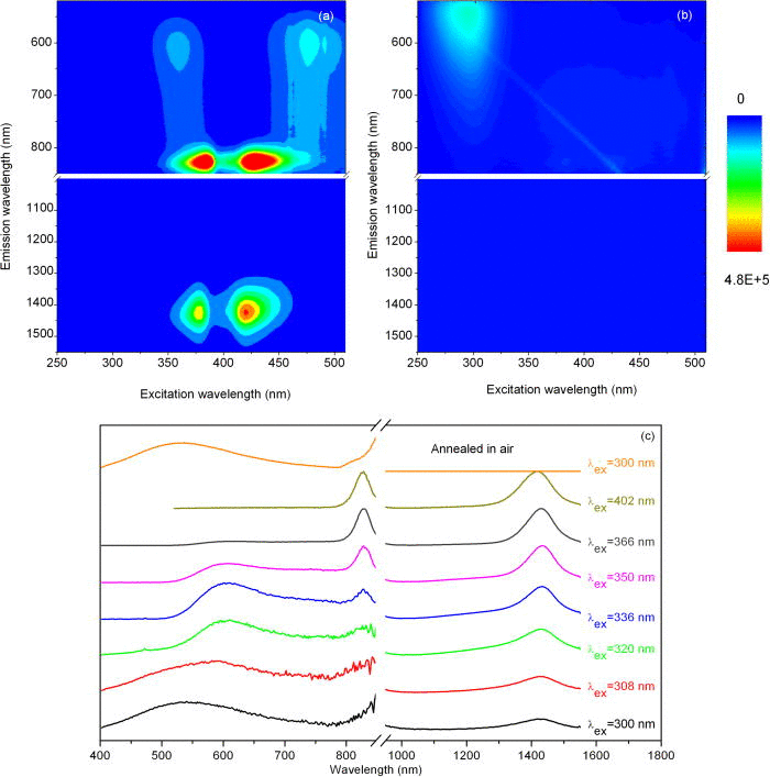 |
Photoluminescence (PL) properties of bismuth (Bi) doped porous silica thin films annealed at various temperatures and in different atmospheres were studied. The near infrared (NIR) luminescence depended strongly on the annealing atmosphere and temperature. To reveal the origin of the NIR luminescence, we performed comprehensive PL studies including steady state and time-resolved PL measurements at 8?300?K in wide excitation (250?500?nm) and detection (400?1550?nm) wavelength ranges. It was revealed that multiple Bi luminescence centers, such as Bi3+, Bi2+, Bi+, and Bi dimer, are stabilized in porous silica. |
| 179. Toshiyuki Kodama, Minoru Fujii, Taishi Nakano, Kenji Imakita, Shinji
Hayashi, "Enhancement of Upconversion Luminescence of Er and Yb Co-doped Y2O3 Nanoparticle by Ag Half-Shell", Optical Materials, Vol. 35, Issue. 12, pp. 2394-2399 (2013). |
|
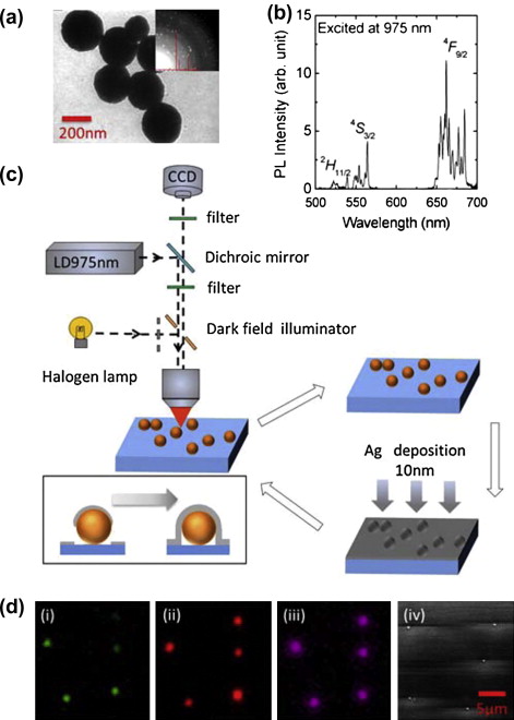 |
Upconversion photoluminescence (PL) properties of single Y2O3 nanoparticles doped with Yb and Er (Y2O3:Yb,Er) with a Ag over-layer is studied. We traced the PL and light scattering images of individual nanoparticles by changing the thickness of a Ag over-layer. When the Ag thickness is relatively small and only the upper part of a nanoparticle is covered by Ag (Ag half-shell), the PL is strongly enhanced. On the other hand, when the Ag thickness is increased and a continuous Ag over layer is formed, the enhancement factor decreases. From the correlation between the enhancement factors of the upconversion PL and scattering intensities as well as the change of the PL lifetime, the mechanism of the PL enhancement is discussed. |
| 178. Hiroshi Sugimoto, Minoru Fujii, Kenji Imakita, Shinji Hayashi, and
Kensuke Akamatsu, "Codoping n- and p-Type Impurities in Colloidal Silicon Nanocrystals -Controlling Luminescence Energy from below Bulk Band Gap to Visible Range", The Journal of Physical Chemistry C, Vol. 117, Issue. 22, pp. 11850-11857 (2013). |
|
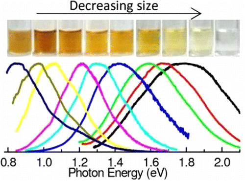 |
We present a novel synthesis of ligand-free colloidal silicon nanocrystals (Si-NCs) that exhibits efficient photoluminescence (PL) in a wide energy range (0.85?1.8 eV) overcoming the bulk Si band gap limitation (1.12 eV). The key technology to achieve the wide-range controllable PL is the formation of donor and acceptor states in the band gap of Si-NCs by simultaneous doping of n- and p-type impurities. The colloidal Si-NCs are very stable in an ordinary laboratory atmosphere for more than a year. Furthermore, the PL spectra are very stable and are not at all affected even when the colloids are drop-cast on a substrate and dried in air. The engineering of the all-inorganic colloidal Si-NC and its optical data reported here are important steps for Si-based optoelectronic and biological applications. |
| 177. Kenji Imakita, Hiroki Shibata, Minoru Fujii, and Shinji Hayashi, "Numerical analysis on the feasibility of a multi-layered dielectric sphere as a three-dimensional photonic crystal", Optics Express, Vol. 2, Issue 9, pp. 10651-10658 (2013). |
|
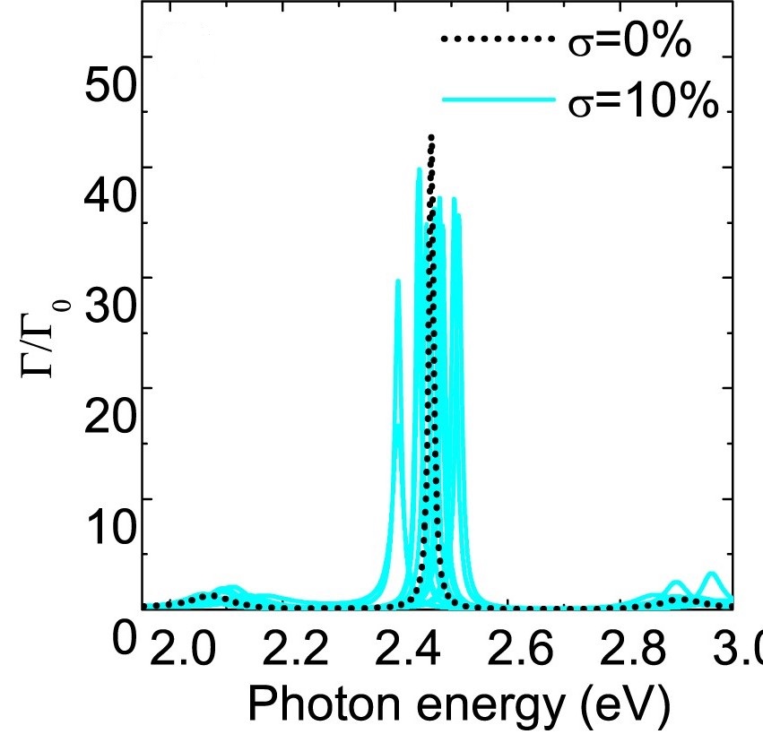 |
The radiative decay rate of a dipole emitter inside the core of a multi-layered dielectric sphere is theoretically investigated. It is shown that, when the thickness of each layer coincides with a quarter wavelength, the multi-layered sphere has a great potential to work as a three-dimensional photonic crystal with a high quality factor and a small mode volume. From the analysis of the dipole position dependence of a radiative decay rate, we show that a smaller core radius, a quarter wavelength at the smallest, is more suitable for real applications. The investigation on the tolerance for thickness nonuniformity reveals that the thickness variation of 10% is tolerable. |
| 176. Batakrushna Santara, Pravat K. Giri, Kenji Imakita, and Minoru Fujii,
"Evidence of Oxygen Vacancy Induced Strong Room Temperature Ferromagnetism in Solvothermally Synthesized Undoped TiO2 Nanoribbons", Nanoscale, Vol. 5, pp. 5476-5488 (2013). |
|
 |
We report on the oxygen vacancy induced ferromagnetism (FM) at and above room temperature in undoped TiO2 nanoporous nanoribbons synthesized by a solvothermal route. The origin of FM in as-synthesized and vacuum annealed undoped nanoribbons grown for different reaction durations followed by calcinations was investigated by several experimental tools. X-Ray diffraction pattern and micro-Raman studies reveal the TiO2(B), TiO2(B)-anatase, and anatase?rutile mixed phases of TiO2 structure. Field emission scanning electron microscopy and transmission electron microscopy observations reveal nanoribbons with uniform pore distribution and nanopits/nanobricks formed on the surface. These samples exhibit strong visible photoluminescence associated with oxygen vacancies and a clear ferromagnetic hysteresis loop, both of which dramatically enhanced after vacuum annealing. Direct evidence of oxygen vacancies and related Ti3+ in the as-prepared and vacuum annealed TiO2 samples are provided through X-ray photoelectron spectroscopy analysis. Micro-Raman, infrared absorption and optical absorption spectroscopic analyses further support our conclusion. The observed room temperature FM in undoped TiO2 nanoribbons is quantitatively analyzed and explained through a model involving bound magnetic polarons (BMP), which include an electron locally trapped by an oxygen vacancy with the trapped electron occupying an orbital overlapping with the unpaired electron (3d1) of Ti3+ ion. Our analysis interestingly shows that the calculated BMP concentration scales linearly with concentration of oxygen vacancies and provides a stronger footing for exploiting defect engineered ferromagnetism in undoped TiO2 nanostructures. The development of such highly porous TiO2 nanoribbons constitutes an important step towards realizing improved visible light photocatalytic and photovoltaic applications of this novel material. |
| 175. Hiroshi Sugimoto, Minoru Fujii, Kenji Imakita, Shinji Hayashi, and
Kensuke Akamatsu, "Phosphorus and Boron Co-doped Colloidal Silicon Nanocrystals with Inorganic Atomic Ligands", The Journal of Physical Chemistry C, Vol. 117, Issue. 13, pp. 6807-6813 (2013). |
|
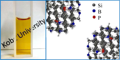 |
The surface structure of P and B codoped colloidal Si-NCs are studied by photoluminescence (PL) in hydrofluoric acid (HF) solution and X-ray photoelectron spectroscopy (XPS). We find that codoped Si-NCs are much more stable in HF solution than undoped, P-doped, and B-doped Si-NCs. The PL study combined with XPS results reveal that a high B concentration layer is formed on the surface of codoped Si-NCs and the layer acts as a kind of inorganic atomic ligands for Si-NCs. The high B concentration layer makes Si-NCs hydrophilic and dispersible in polar liquids. Furthermore, the layer effectively protects Si-NCs from oxidation in solution and in air. |
| 174. Zhenhua Bai, Minoru Fujii, Kenji Imakita, and Shinji Hayashi,
Green to Red Tunable Upconversion Fluorescence from Bi-Er-Yb Codoped Zeolites Microporous and Mesoporous Materials, Vol. 173, pp. 43-46 (2013). |
|
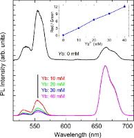 |
We investigate the infrared-to-visible upconversion (UC) fluorescence properties of Bi?Er?Yb codoped zeolites. It is revealed that the UC emissions can be well controlled by the Yb3+ concentration in zeolites. By the addition of Yb3+, the green and red emissions are enhanced about 5 and 243 times, respectively. On the other hand, the intensity ratio of red-to-green is increased from 0.26 to 12.2. The tunable emission is due to the energy back transfer from Yb3+ to Er3+. It is expected that the achieved intense single band red emission may have potential application for in vivo bioimaging. |
| 173. Jiajia Zhou, Naoto Shirahata, Hong-Tao Sun, Batu Ghosh, Makoto Ogawara,
Yu Teng, Shifeng Zhou, Rong Gui Sa Chu, Minoru Fujii, and Jianrong Qiu,
Efficient Dual-Modal NIR-to-NIR Emission of Rare Earth Ions Co- doped Nanocrystals for Biological Fluorescence Imaging The Journal of Physical Chemistry Letters, Vol. 4, pp. 402-408 (2013). |
|
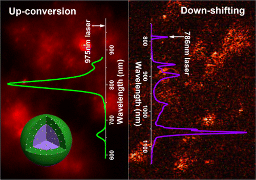 |
A novel approach has been developed for the realization of efficient near-infrared to near-infrared (NIR-to-NIR) upconversion and down-shifting emission in nanophosphors. The efficient dual-modal NIR-to-NIR emission is realized in a β-NaGdF4/Nd3+@NaGdF4/Tm3+?Yb3+ core?shell nanocrystal by careful control of the identity and concentration of the doped rare earth (RE) ion species and by manipulation of the spatial distributions of these RE ions. The photoluminescence results reveal that the emission efficiency increases at least 2-fold when comparing the materials synthesized in this study with those synthesized through traditional approaches. Hence, these core?shell structured nanocrystals with novel excitation and emission behaviors enable us to obtain tissue fluorescence imaging by detecting the upconverted and down-shifted photoluminescence from Tm3+ and Nd3+ ions, respectively. The reported approach thus provides a new route for the realization of high-yield emission from RE ion doped nanocrystals, which could prove to be useful for the design of optical materials containing other optically active centers. |
| 172. Minoru Fujii, Taishi Nakano, Kenji Imakita, and Shinji Hayashi, Upconversion Luminescence of Er and Yb Co-Doped NaYF4 Nanoparticles with Metal Shells The Journal of Physical Chemistry C, Vol. 117, pp. 1113-1120 (2013). |
|
 |
Upconversion photoluminescence (PL) of a composite nanoparticle consisting of an Er and Yb codoped NaYF4 core and a Au shell is studied theoretically and experimentally. We first investigate the effects of a Au shell on the radiative and nonradiative emission rates of a dipole placed in a core, the absorption and scattering cross sections of a composite nanoparticle, and the electric field within a core at the excitation wavelength. We then synthesize the composite nanoparticle and study the PL properties. From the analyses of the PL data in combination with the data obtained by theoretical calculations, the mechanism of the enhancement and quenching of upconversion PL by the formation of a Au shell is studied. |
| 171. Shinsuke Shichi, Minoru Fujii, Kenji Imakita, and Shinji Hayashi,
Porous Silica True Zero-Order Wave Plate in the Deep Ultraviolet Range Optics Communications, Vol.287, pp.137-139 (2013). |
|
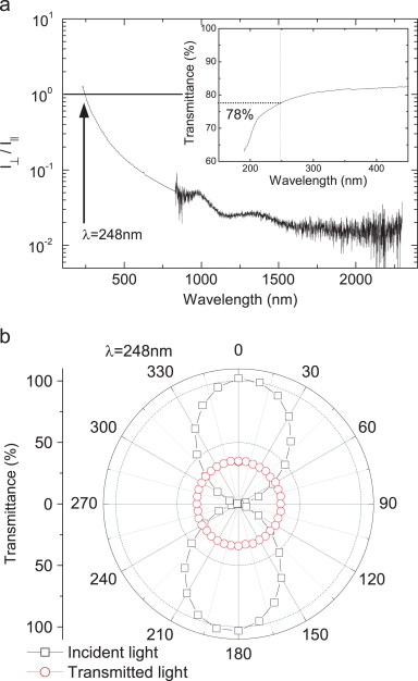 |
True zero-order wave plates operating in the deep ultraviolet (DUV) range are produced from porous silica having very small in-plane optical anisotropy (refractive index anisotropy: ?0.001). Small temperature (4.3×10?5 λ/°C) and angle-dependent shifts of the retardance are obtained in the DUV range. The retardance shifts are 0.007λ and 0.035λ when the plate is tilted 15° on the [0 0 1] and axes, respectively. From the angle dependence, the shape of the refractive index ellipsoids is discussed. |
| 170. Kenji Imakita, Yuya Tsuchihashi, Ryo Naruiwa, Minoru Fujii, Hong-Tao
Sun, Jianrong Qiu, and Shinji Hayashi, "Ultrafast Nonlinear Optical Responses of Bismuth Doped Silicon-Rich Silica Films", Applied Physics Letters, Vol. 101, Issue 19, 191106, pp. 1-4 (2012). |
|
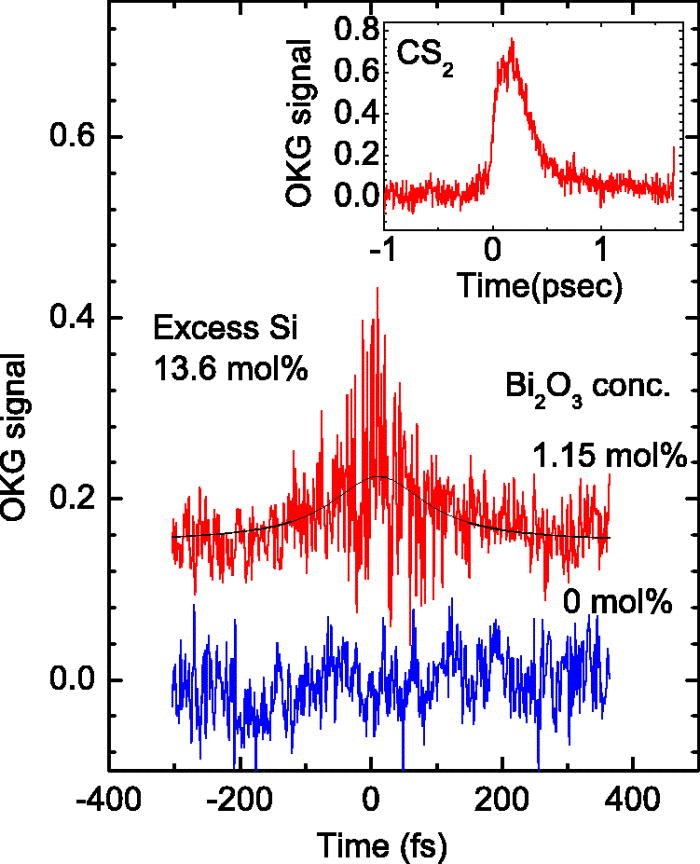 |
Nonlinear optical responses of bismuth (Bi) doped silicon-rich silicon dioxide (Si-rich SiO2) films were studied by a z-scan and an optical Kerr gate method under femtosecond excitation around 800?nm. It was found that the Bi-doping enhances the nonlinear optical response of Si-rich SiO2 films by several orders of magnitudes. The nonlinear refractive index was of the order of 10?11?cm2/W and the response time was shorter than our time resolution of 100 fs. The nonlinear refractive index was independent of the wavelength in the range from 750 to 835?nm, suggesting that virtual transitions are involved in the nonlinear optical processes. |
| 169. Hong-Tao Sun, Yoshio Sakka, Naoto Shirahata, Minoru Fujii, and Tetsu
Yonezawa, Near-infrared photoluminescence from molecular crystals containing tellurium Journal of Materials Chemistry, Vol. 22, pp. 24792-24797 (2012). |
|
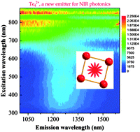
|
We report the observation of near-infrared photoluminescence from Te4(Ga2Cl7)2 and Te4(Al2Cl7)2 molecular crystals containing Te42+ polycations. The experimental and theoretical results clearly revealed that the Te42+ polycation is a smart near-infrared emitter with characteristic emission peaks at 1252 and 1258 nm for Te4(Ga2Cl7)2 and Te4(Al2Cl7)2 crystals, respectively, resulting from the intrinsic electronic transitions of Te42+. Furthermore, it was also found that the emissions strongly depend on the excitation wavelengths for both Te4(Ga2Cl7)2 and Te4(Al2Cl7)2 samples, most possibly due to the co-existence of other Te-related optically active centers. This research not only enriches the species of luminescent charged p-block element polyhedra and deepens the understanding of Te-related photophysical behaviors, but also may stimulate efforts for designing novel material systems using such active centers. It is also greatly expected that these sub-nanometer optically active species could exist in other systems such as glasses, polymers, and bulk optical crystals, and the stabilization of these centers in widely used hosts will pave the way for their practical applications. |
| 168. Kei Ueda, Takeshi Tayagaki, Masatoshi Fukuda, Minoru Fujii, and Yoshihiko
Kanemitsu, Breakdown of the k-conservation Rule in Quantized Auger Recombination in Si1-xGe |
|
 |
Dynamics of quantized Auger recombination in Si1?xGex nanocrystals (NCs) embedded in SiO2 films was studied by femtosecond intraband pump-probe spectroscopy. The temporal change of the electron-hole pair number under strong photoexcitation was well explained by the quantized Auger recombination model that considered the size distribution of NCs. On the basis of the dependence of the Auger decay rate on temperature and Ge composition, we confirmed the occurrence of breakdown of the k-conservation rule in quantized Auger recombination in Si and Si1?xGex NCs. |
| 167. Satoshi Morimoto, Minoru Fujii, Hong-Tao Sun, Yuji Miwa, Kenji Imakita,
Jianrong Qiu, and Shinji Hayashi, Broadband Near-Infrared Emission from Bismuth-Doped Multilayer Films Journal of Applied Physics, Vol. 112, 073511, pp. 1-4 (2012). (Copyright (2012) American Institute of Physics. This article may be downloaded for personal use only. Any other use requires prior permission of the author and the American Institute of Physics. ) |
|
 |
Multilayer structures consisting of bismuth (Bi)-doped silica thin films and different kinds of spacer, i.e., Si, silica, Si-rich silica, layers are grown and the luminescence properties are studied. When samples were annealed at a low temperature, Bi-related near infrared active centers (BRACs) were formed at interfaces between Bi-doped silica and Si-rich silica (or silicon) due to the reduction of Bi3+ to BRACs by silicon. On the other hand, films annealed at a high temperature showed similar emission behaviors to bulk glasses. The results demonstrated here establish a new strategy for the control of BRACs and building peculiar Bi activated film structures. |
| 166. Hong-Tao Sun, Tetsu Yonezawa, Miriam M. Gillett-Kunnath, Yoshio Sakka,
Naoto Shirahata, Sa Chu Rong Gui, Minoru Fujii and Slavi C. Sevov, Ultra-Broad Near-Infrared > tolu>inescence from Crystalline (K-crypt)2Bi2 Containing [Bi2]2- Dimers Journal of Materials Chemistry, Vol.22, Issue 38, pp. 20175-20178 (2012). |
|
 |
For the first time, we report that a single crystal of (K-crypt)2Bi2 containing [Bi2]2? displays ultra-broad near-infrared photoluminescence (PL) peaking at around 1190 nm and having a full width at the half maximum of 212 nm, stemming from the inherent electronic transitions of [Bi2]2?. The results not only add to the number of charged Bi species with luminescence, but also deepen the understanding of Bi-related near-infrared emission behavior and lead to the reconsideration of the fundamentally important issue of Bi-related PL mechanisms in some material systems such as bulk glasses, fibers, and conventional optical crystals. |
| 165. Hong-Tao Sun, Beibei Xu, Tetsu Yonezawa, Yoshio Sakka, Naoto Shirahata,
Minoru Fujii,Jianrong Qiu and Hong Gao, Photoluminescence from Bi5(GaCl4)3 Molecular Crystal Dalton Transactions, Vol. 41, pp.11055-11061 (2012). |
|
 |
Bi5(GaCl4)3 sample has been synthesized through the oxidation of Bi metal by gallium chloride (GaCl3) salt. Powder X-ray diffraction as well as micro-Raman scattering results revealed that, in addition to crystalline Bi5(GaCl4)3 in the product, an amorphous phase containing [GaCl4]? and [Ga2Cl7]? units also exists. The thorough comparison of steady-state and time-resolved photoluminescent behaviors between the Bi5(GaCl4)3 product and Bi5(AlCl4)3 crystal leads us to conclude that Bi53+ is the dominant emitter in the product, which gives rise to the ultrabroad emission ranging from 1 to 2.7 μm. Detailed quantum chemistry calculation helps us assign the observed excitations to some electronic transitions of the Bi53+ polycation, especially at shorter wavelengths. It is believed that our work shown here is not only helpful to solve the confusions on the luminescent origin of bismuth in other material systems, but also serves to develop novel broadband tunable laser materials. |
| 164. Hiroshi Sugimoto, Minoru Fujii, Kenji Imakita, Shinji Hayashi,and
Kensuke Akamatsu, All-Inorganic Near-Infrared Luminescent Colloidal Silicon Nanocrystals-High Dispersibility in Polar Liquid by Phosphorus and Boron Co-doping The Journal of Physical Chemistry C., Vol.116, Issue. 33, pp.17969-17974 (2012). |
|
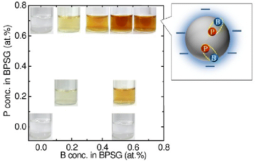 |
We demonstrate the formation of a new type of surfactant-free colloidal silicon nanocrystal (Si-NC). The characteristic structural feature of the Si-NCs is simultaneous doping of phosphorus (P) and boron (B) in and on the surface of Si-NCs. The codoped Si-NCs are stable in methanol for more than a year and exhibit luminescence in the near-infrared range. We perform comprehensive studies on the structure of codoped colloidal Si-NCs and discuss the mechanism of the high solution dispersibility. |
| 163. Kenji Imakita, Masahiko Ito, Ryo Naruiwa, Minoru Fujii, and Shinji
Hayashi, Ultrafast Third Order Nonlinear Optical Response of Donor and Acceptor Codoped and Ccompensated Silicon Quantum Dots Applied Physics Letters, Vol. 101(4), 041112, pp. 1-3 (2012). |
|
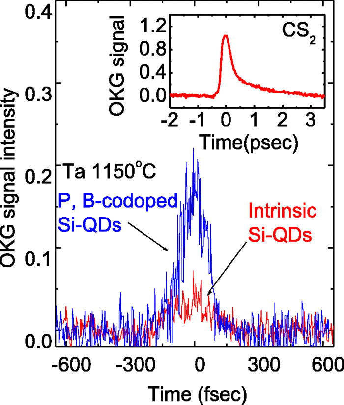 |
Nonlinear optical responses of phosphorus and boron codoped and compensated silicon quantum dots (Si-QDs) embedded in borophosphosilicate glass were studied by a z-scan and an optical Kerr gate methods under femtosecond excitation at 780?nm. The nonlinear refractive index (n2) and the two photon absorption coefficients (β) of compensated Si-QDs were found to be enhanced several times compared to those of intrinsic Si-QDs. The response time was shorter than our time resolution of 100?fs at room temperature. |
| 162. Shinji Hayashi, Yuta Ishigaki, and Minoru Fujii, Plasmonic Effects on Strong Exciton-Photon Coupling in Metal-Insulator-Metal Microcavities Physical Review B, Vol. 86, 045408, pp. 1-8 (2012). |
|
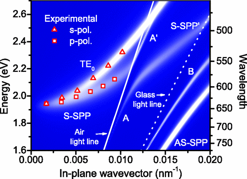 |
Metal-insulator-metal (MIM) microcavities consisting of a layer of polyvinyl alcohol doped and undoped with cyanine dye molecules were prepared and their reflection and transmission spectra were measured. In the doped-MIM microcavity, dispersion curves determined from the reflection data clearly showed the anticrossing behavior arising from the strong coupling between excitons in the dye molecules and photonic modes supported by the MIM microcavity. The experimental dispersion curves could be well reproduced by a standard expression of the coupled mode dispersions by appropriately taking into account the plasmonic nature of the transverse magnetic mode supported by the MIM microcavity. A large splitting between the transverse electric and transverse magnetic modes in the upper branch of the coupled modes can also be well explained by the plasmonic effects. |
| 161. Kenji Imakita, Masahiko Ito, Ryo Naruiwa, Minoru Fujii, and Shinji
Hayashi, Enhancement of Ultrafast Nonlinear Optical Response of Silicon Nanocrystals by Boron-Doping Optics Letters, Vol. 37, No. 11, pp. 1877-1879 (2012). |
|
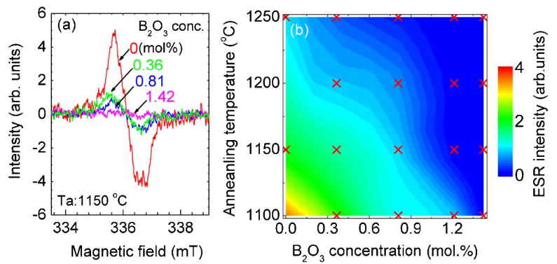 |
Nonlinear optical responses of boron (B)-doped silicon nanocrystals (Si-ncs) embedded in borosilicate glass were studied by z-scan and optical Kerr gate methods under femtosecond excitation at 780 nm. The nonlinear refractive index ( 2) and the two photon absorption coefficients ( ) of B-doped Si-ncs were found to be 3 times enhanced, compared to those of intrinsic Si-ncs. The response time was faster than 100 fs even at 5 K. The origin of the large nonlinear optical response was discussed, based on the experimental data of 2, electron spin resonance spectra, and linear absorption spectra. |
| 160. Shinsuke Shichi, Minoru Fujii, Tomoki Nishida, Hidehiro Yasuda, Kenji
Imakita, and Shinji Hayashi, Three-Dimensional Structure of (110) Porous Silicon with In-Plane Optical Birefriengence Journal of Applied Physics, Vol. 111, 084303, pp. 1-6 (2012). (Copyright (2012) American Institute of Physics. This article may be downloaded for personal use only. Any other use requires prior permission of the author and the American Institute of Physics. ) |
|
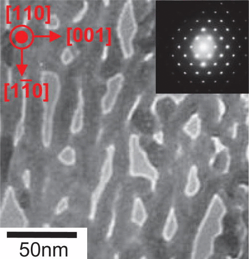 |
Electrochemical etching of a (110) oriented Si wafer results in a porous silicon (PSi) layer which exhibits a strong in-plane optical birefringence. We study the refractive index ellipsoid of (110) PSi by angle-resolved optical transmittance measurements and reveal that it is a biaxial crystal. The angle-resolved transmission electron microscope observations demonstrate that pores grow along the directions in between the <100> crystal axes and the etching current flow and these directions depend on the etching current density. The etching current density dependence of the pore direction indicates that the shape of the index ellipsoid can be controlled by the etching condition. |
| 159. Sa chu rong gui, Kenji Imakita, Minoru Fujii, Zhenhua Bai, Shinji
Hayashi, Luminescence Properties of Bi-Doped Oxidized Porous Silicon Thin Films Optical Materials, Vol. 34, pp. 1161-1164 (2012). |
|
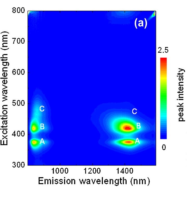 |
Luminescence properties of Bi-doped oxidized porous silicon (OPS) thin films were studied. It was found that this material shows two broad luminescence bands centered at 845 nm with the FWHM of 120 nm and at 1410 nm with that of 220 nm under 488 nm excitation. A detailed analysis of the 3D plot of PL intensities versus excitation and emission wavelengths revealed that these luminescence bands arise from at least two different kinds of Bi luminescence centers. The broad luminescence covering the whole telecommunication window (1.2?1.6 μm) suggests that Bi-doped OPS thin films can be a candidate material for a broadband waveguide-type optical amplifier at optical telecommunication wavelengths. |
| 158. Toshihiro Nakamura, Sadao Adachi, Minoru Fujii, Kenta Miura, and Shunya
Yamamoto, Phosphorus and Boron Codoping of Silicon Nanocrystals by Ion Implantation: Photoluminescence Properties Physical Review B, Vol. 85, 045441, pp.1-7 (2012). |
|
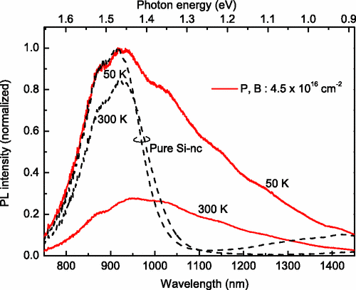 |
The photoluminescence (PL) properties of P or B single-doped Si nanocrystals (Si-nc's) and P and B co-doped Si-nc's are studied. In the single-doped Si-nc samples, PL quenching occurs as a result of the Auger nonradiative recombination process between the photoexcited excitons and free carriers supplied by doped impurities. In the (P, B) co-doped sample, on the other hand, the donor-acceptor (D-A)-pair recombination emission is clearly observed on the long-wavelength side of the intrinsic Si-nc emission peak at ?900 nm. The D-A-pair recombination energy is found to be smaller than the band-gap energy of bulk Si and is strongly dependent on the number of P and B impurities doped in a Si-nc. PL spectra are measured at 50 and 300 K and found to indicate that strong thermal quenching occurs in a (P, B) co-doped sample at 300 K. This quenching effect is probably because of carrier migration among the donor and acceptor states. The PL decay rate is determined as a function of the emitted-light wavelength for the pure and (P, B) co-doped Si-nc samples. |
| 157. Koji Matsuhisa, Minoru Fujii, Kenji Imakita, and Shinji Hayashi, Photoluminescence from Single Silicon Quantum Dots Excited via Surface Plasmon Polaritons Journal of Luminescence, Vol. 132, pp. 1157-1159 (2011). |
|
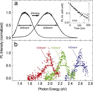 |
Single dot spectroscopy of Si quantum dots (QDs) was performed by using surface plasmon polariton (SPP)-mediated excitation in the attenuated total reflection geometry with a MgF2/Ag film on the base of a prism. Thanks to the 16 times enhancement of the incident electric field and very small background signal, PL from single Si QDs was observed clearly. This proves the usefulness of the technique for the detection of inherently weak emission of Si QDs. |
| 156. Zhenhua Bai, Minoru Fujii, Takashi Hasegawa, Shohei Kitanoa, Kenji
Imakita, Minoru Mizuhatab, and Shinji Hayashi, Co-existence of Bi with Multiple Valence States in Zeolites -Controlling the Optical Properties by Annealing Atmosphere Optical Materials, Vol. 34 , pp. 821-825 (2011). |
|
 |
We investigate the effect of annealing atmosphere on the optical properties of Bi doped zeolites by diffuse reflectance, steady state and time-resolved photoluminescence (PL), and PL excitation measurements. The results reveal that zeolites can be used as an excellent host material to stabilize multiple Bi centers (Bi3+, Bi2+, and Bi-related near-infrared (NIR) active centers) in the framework, which shows ultra-broadband emission from visible to NIR range. Annealing in N2 leads to the partial conversion of Bi3+ ions into Bi2+ and Bi-related NIR active centers. Our results demonstrate that the broadband NIR emission may be attributed to the electronic transition of Bi low valence state, rather than a higher valence state. |
| 155. Ilya Sychugov, Jan Valenta, K. Mitsuishi, Minoru Fujii, and Jan Linnros,
Photoluminescence Measurements of Zero-Phonon Optical Transitions in Silicon Nanocrystals Physical Review B, Vol. 84, 125326, pp. 1-5 (2011). |
|
|
Optical transitions in silicon nanocrystals with different surface passivations were probed at low temperatures on a single-particle level. A type of quasidirect recombination process, different from the quantum-confined exciton transition, is identified. The luminescence spectra have different emission energies, but the contribution of a no-phonon transition is significantly higher than expected from the quantum-confinement model. Its relative strength was found to be temperature dependent, suggesting spatial localization of excitons as a possible origin. |
| 154. Yuji Miwa, Hong-Tao Sun, Kenji Imakita, Minoru Fujii, Yu Teng, Jianrong
Qiu, Yoshio Sakka, and Shinji Hayashi, Sensitized Broadband Near-Infrared Luminescence from Bismuth-Doped Silicon-Rich Silica Films Optics Letters, Vol. 36, No. 21, pp. 4221-4223, November 1 (2011). |
|
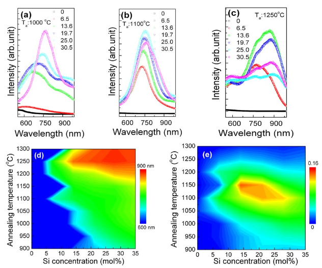 |
Developing Si compatible optical sources has attracted a great deal of attention owing to the potential for forming inexpensive, monolithic Si-based integrated devices. In this Letter, we show that ultra broadband near-IR (NIR) luminescence in the optical telecommunication window of silica optical fibers was obtained for Bi-doped silicon- rich silica films prepared by a co-sputtering method. Without excess Si, i.e., Bi-doped pure silica films, no luminescence was observed in the NIR range. A broad Bi-related NIR photoluminescence appears when excess Si was doped in the Bi-doped silica. The luminescence properties depended strongly on the amount of excess Si and the annealing temperature. Photoluminescence results suggest that excess Si acts as an agent to activate Bi NIR luminescence centers and also as an energy donor to transfer excitation energy to the centers. It is believed that this peculiar structure might find some important applications in Si photonics. |
| 153. Zhenhua Bai, Minoru Fujii, Takashi Hasegawa, Kenji Imakita,Minoru
Mizuhata and Shinji Hayashi, Efficient Ultraviolet-Blue to Near-Infrared Downconversion in Bi-Dy-Yb Doped Zeolites Journal of Physics D: Applied Physics, Vol. 44, pp. 455301 1-5 (2011). |
|
 |
Ultraviolet-blue to near-infrared (NIR) downconversion is investigated for the Dy3+?Yb3+ couple in zeolites by steady-state and time-resolved photoluminescence (PL) spectra, and PL excitation spectra. Upon excitation of the 4F9/2 level of Dy3+, NIR quantum cutting could occur through a two-step energy transfer from one Dy3+ ion to two neighbouring Yb3+ ions via an intermediate level. The energy transfer efficiency from the 4F9/2 level is estimated to be 42%, and the intrinsic PL quantum efficiency of Yb3+ emission reaches 54%. The findings may have potential application in enhancing the energy efficiency of silicon-based solar cells. |
| 152. Masatoshi Fukuda, Hiroshi Sugimoto, Minoru Fujii, Kenji Imakita, and
Shinji Hayashi, Surfactant-Free Solution-Dispersible Si Nanocrystals -Surface Modification by Impurity Control Optics Letters, Vol. 36, No. 20, pp. 4014-4016 (2011). |
|
|
Si nanocrystals (Si-NCs) dispersible in polar liquid without surface functionalization by organic molecules have been realized by simultaneously doping n and p type impurities. We show that the codoped Si-NCs are stable in methanol for more than five months, while intrinsic Si-NCs prepared by the same procedure form large agglomerates. The different behavior of the intrinsic and codoped Si-NCs in solutions suggests that doped impurities exist on the surface of Si-NCs and the surface potential is large enough to prevent the agglomeration. The colloidal solution of codoped Si-NCs exhibits broad photoluminescence with the maximum in the near infrared range (1.1?1.3?eV). |
| 151. Shinsuke Shichi, Minoru Fujii, and Shinji Hayashi, Ultraviolet True Zero-Order Wave Plate Made of Birefringent Porous Ssilica Optics Letters, Vol. 36, No. 19, pp. 3951-3953 (2011). |
|
|
Porous Si made from (110) Si wafers exhibits strong in-plane optical anisotropy (birefringence) in the visible and near-IR ranges. Oxidation of the birefringent porous Si results in the formation of birefringent porous silica. We demonstrate that the degree of the birefringence of porous silica can be controlled by the oxidation condition, and very small birefringence can be achieved. The smallest anisotropy of the refractive index (Δ ) is 0.001, which is about ten times smaller than that of quartz. The small birefringence allows us to produce true zero-order wave plates operating in the UV range. |
| 150. Hiroshi Sugimoto, Minoru Fujii, Masatoshi Fukuda, Kenji Imakita, and
Shinji Hayashi, Acceptor-Related Low-Energy Photoluminescence from Boron-Doped Si Nanocrystals Journal of Applied Physics, Vol. 110, 063528, pp. 1-6 (2011). (Copyright (2011) American Institute of Physics. This article may be downloaded for personal use only. Any other use requires prior permission of the author and the American Institute of Physics. ) |
|
|
Boron (B) doped Si nanocrystals (Si-ncs) dispersed in hydrofluoric (HF) acid solution are prepared by dissolving borosilicate films containing B-doped Si-ncs in HF solution. We find that the etching rate of B-doped Si-ncs is much smaller than that of undoped Si-ncs. The difference of the etching rate allows us to extract only doped Si-ncs in the mixture of doped and undoped Si-ncs and observe the photoluminescence (PL) due to the transition from the conduction band to the acceptor state. The PL was very broad with the maximum around 1.15 eV. From the analysis of the PL data obtained for the samples prepared under different conditions and different etching time, preferential doping sites of B atoms are estimated. The data suggests that B-doped Si-ncs consists of intrinsic cores and heavily B-doped shells. |
| 149. Yohei Takeichi, Yasuo Kimoto, Minoru Fujii, and Shinji Hayashi Anisotropic Propagation of Surface Plasmon Polaritons Induced by Para-Sexiphenyl Nanowire Films Physical Review B, Vol. 84, 085417 pp. 1-7 (2011). |
|
|
Thin films of aligned nanowires composed of oriented para-sexiphenyl molecules were prepared on muscovite mica substrates and transferred to the surfaces of Ag films. Results of attenuated total reflection (ATR) measurements on these samples with a fixed wavelength of incident light clearly demonstrate the anisotropic propagation of surface plasmon polaritons (SPPs) induced by the optical anisotropy in the nanowire films. The magnitude of the SPP wave vector takes a maximum value when the SPP propagates along the direction of molecular orientation. Results of ATR measurements performed for various wavelengths of the incident light reveal the anisotropy in the SPP dispersion curve in a wide range of photon energy. From the fitting of theoretical reflection curves to observed ATR spectra, dispersions of the principal values of dielectric tensor of the nanowire film are obtained. |
| 148. Shu Okada, Minoru Fujii, and Shinji Hayashi Immobilization of polyynes adsorbed on Ag nanoparticle aggregates into poly(vinyl alcohol) films Carbon, Vol. 49, pp. 4704-4709 (2011). |
|
|
Thin films of aligned nanowires composed of oriented para-sexiphenyl molecules were prepared on muscovite mica substrates and transferred to the surfaces of Ag films. Results of attenuated total reflection (ATR) measurements on these samples with a fixed wavelength of incident light clearly demonstrate the anisotropic propagation of surface plasmon polaritons (SPPs) induced by the optical anisotropy in the nanowire films. The magnitude of the SPP wave vector takes a maximum value when the SPP propagates along the direction of molecular orientation. Results of ATR measurements performed for various wavelengths of the incident light reveal the anisotropy in the SPP dispersion curve in a wide range of photon energy. From the fitting of theoretical reflection curves to observed ATR spectra, dispersions of the principal values of dielectric tensor of the nanowire film are obtained. |
| 147. Zhenhua Bai, Minoru Fujii, Takashi Hasegawa, Kenji Imakita, Yuji Miwa,
Minoru Mizuhata, and Shinji Hayashi Effect of doping concentration on broadband near-infrared emission of Bi doped zeolites Microporous and Mesoporous Materials, Vol. 145, pp. 21-25 (2011). |
|
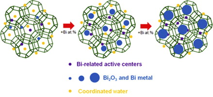 |
A series of Bi doped zeolites are prepared by an ion-exchange process by changing doping concentration in a wide range, and the optical properties are investigated. The near-infrared photoluminescence (PL) intensity, full width at half maximum and decay time depend strongly on Bi doping concentration. The PL intensity increases 178 times when the concentration is changed from 0.3 to 1.5 at. %. At the same time, the lifetime increases from 83 to 527 μs. The results prove the model that doped Bi acts not only as optically active centers, but also as pore-sealing substances to isolate the centers. The comparison of PL and Raman data suggests that in addition to previously proposed Bi2O3, other Bi-related materials, probably Bi metal, play an important role to isolate the active centers. |
| 146. Hong-Tao Sun, Yoshio Sakka, Hong Gao, Yuji Miwa, Minoru Fujii, Naoto
Shirahata, Zhenhua Bai and Ji-Guang Li, Ultrabroad near-infrared photoluminescence from Bi5(AlCl4)3 crystal Journal of Materials Chemistry, Vol. 21, pp. 4060-4063 (2011). |
|
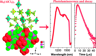 |
The Bi5(AlCl4)3 crystal, synthesized by a environmentally friendly room-temperature method using ionic liquids as reaction solvents, exhibits extremely broad near-infrared photoluminescence (PL) with a full width at the half maximum (FWHM) of >510 nm and an effective PL lifetime of 4.1 μs at 1160 nm. We envision that this study not only extends the understanding of photophysical properties of materials containing subvalent bismuth, but also may have promise for the design of novel photonic materials containing a wide array of p-block elements. |
| 145. Zhenhua Bai, Hong-Tao Sun, Minoru Fujii, Yuji Miwa,Takashi Hasegawa,
Minoru Mizuhata and Shinji Hayashi, Bismuth-sensitized Efficient Near-infrared Luminescence from Ytterbium in Zeolites Journal of Physics D: Applied Physics, Vol. 44, 155101, pp. 1-5 (2011). |
|
 |
Yb?Bi co-doped zeolites are prepared by a method consisting of a simple ion-exchange process and subsequent high-temperature annealing. We observe two strong near-infrared (NIR) emission bands overlapping in the range 930?1480?nm, corresponding to the electronic transitions of bismuth-related active centres (BiRAC) and Yb3+ ions, respectively. In the obtained products, the excitation wavelength of Yb3+ is extended to the range 420?850?nm, and the lifetime reaches 665?μs. In the zeolite matrix, Bi ions exist as BiRAC and Bi compound agglomerates. The former act as a sensitizer of Yb3+ ions, and the latter act as a blockage to seal the pores of zeolites, which enables Yb3+ ions to show efficient NIR emission even if the zeolites contain a large amount of coordinated water. The excellent optical and structural properties make these NIR-emitting nanoparticles promising in applications as biological probes. |
| 144. Zhenhua Bai, Minoru Fujii, Yuki Mori, Yuji Miwa, Minoru Mizuhata,
Hong-Tao Sun, and Shinji Hayashi, Efficient Near-infrared Emission from Neodymium by Broadband Sensitization of Bismuth in Zeolites Optics Letters, Vol. 36, No. 6, pp. 1017-1019 (2011) . |
|
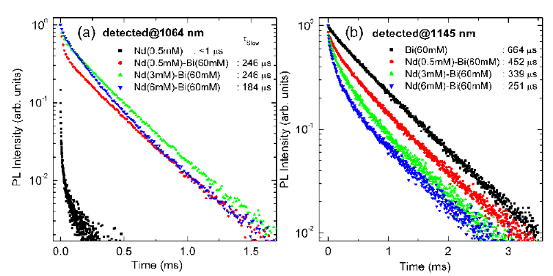 |
Nd-Bi codoped zeolites were prepared by an ion-exchange process, and the optical properties were investigated by photoluminescence (PL) and PL excitation spectra, and decay time measurements. The results show that the NIR emission of Nd3+ ions is significantly enhanced by the introduction of bismuth in codoped samples, and the lifetime reaches 246?μs. It is also observed that NIR-active Bi acts as a sensitizer of Nd3+ ions. The energy transfer efficiency is also estimated. The peculiar optical properties make Nd-Bi codoped zeolites promising for potential application in biological probes. |
| 143. Masatoshi Fukuda, Minoru Fujii, and Shinji Hayashi, Room-temperature below Bulk-Si Band Gap Photoluminescence from P and B Co-doped and Compensated Si Nanocrystals with Narrow Size Distributions Journal of Luminescence, Vol. 131, Issue 5, pp. 1066-1069 (2011) . |
|
 |
Thin films consisting of the layers of phosphorus (P) and boron (B) co-doped Si nanocrystals (Si-ncs) and glass spacer layers were prepared and their photoluminescence properties were studied. Cross-sectional TEM observations revealed the growth of Si-ncs with narrow size distributions. The samples exhibited PL below the band gap energy of bulk Si crystal at room temperature. The low-energy PL is considered to arise from the transitions between donor and acceptor states in compensated Si-ncs. The successful formation of narrow size distribution co-doped Si nanocrystals promotes the study of the optical properties of compensated Si nanocrystals. |
| 142. Kenji Hanamura, Minoru Fujii, Tomonari Wakabayashi, and Shinji Hayashi, Surface-enhanced Raman Scattering of Size-selected Polyynes (C8H2) Adsorbed on Silver Colloidal Nanoparticles Chemical Physics Letters, Vol. 503, No. 1-3, pp. 118-123 (2011) . |
|
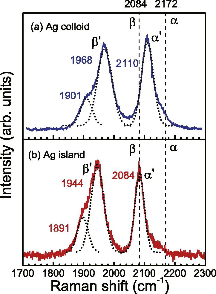 |
Absorption and surface-enhanced Raman scattering (SERS) spectra of size-selected C8H2 adsorbed on Ag colloids were investigated. The Ag colloids after C8H2 adsorption are stable without precipitation of Ag nanoparticle aggregates. The spectra strongly depend on the C8H2 concentration. A good correlation between the concentration dependence of the absorption spectrum and that of SERS intensities supports the electromagnetic mechanism of SERS. The use of size-selected C8H2 made it possible to demonstrate also the chemical effects, which manifest themselves in the differences in the positions of SERS bands for different SERS enhancers, i.e., Ag colloid and Ag island film. |
| 141. Hong-Tao Sun, Junjie Yang, Minoru Fujii, Yoshio Sakka, Yufang Zhu,
Takayuki Asahara, Naoto Shirahata, Masaaki Ii, Zhenhua Bai, Ji-Guang Li,
and Hong Gao, Highly Fluorescent Silica-Coated Bismuth-Doped Aluminosilicate Nanoparticles for Near-Infrared Bioimaging Small, Vol. 7, No. 2, pp. 199-203 (2011) . |
|
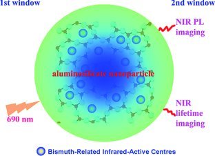 |
The combined advantages of bismuth and aluminosilicates lead to a new type of nanosized biolabel. The near‐infrared (NIR)‐emitting silica‐coated bismuth‐doped aluminosilicate nanoparticles are simple to prepare and exhibit a broad excitation band in the first biological window, efficient long‐lived photoluminescence (PL) covering the second window, high photostability, low cytotoxicity, and easy penetration into living tissues. In vivo PL bioimaging and decay are tested in living mice. |
| 140. Hong-Tao Sun, Yoshio Sakka, Minoru Fujii, Naoto Shirahata, and Hong
Gao, Ultrabroad Near-infrared Photoluminescence from Ionic Liquids Containing Subvalent Bismuth Optics Letters, Vol. 36, No. 2, pp. 100-102 (2011) . |
|
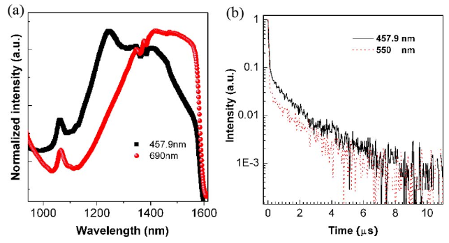 |
We have shown that Lewis-acidic halogenoaluminate ionic liquid (IL) containing subvalent bismuth can be used as a near-IR (NIR) luminescent material. Raman and absorption spectra evidence the coexistence of Bi3+5 and Bi+ in the liquid. The Bi3+5 and Bi+ emitters, stabilized by this Lewis-acidic liquid, demonstrate ultrabroad NIR photoluminescence with a lifetime of around 1μs. We envisage that the bismuth activated ILs would not only enrich the well-established spectrum of soft luminescent materials but also might promote the design of novel photonic materials activated by other p-block elements. |
| 139. Sergej Polisski, Bernhard Goller, Susannah C. Heck, Stefan A. Maier, Minoru
Fujii, and Dmitri Kovalev Formation of Metal Nanoparticles in Silicon Nanopores: Plasmon Resonance Studies Applied Physics Letters, Vol. 98, 011912 pp. 1-3 (2011).(Copyright (2011) American Institute of Physics. This article may be downloaded for personal use only. Any other use requires prior permission of the author and the American Institute of Physics. ) |
|
 |
We present a method for the formation of noble metal nanoparticle ensembles in nanostructured silicon. The key idea is based on the unique property of the large reduction potential of extended internal hydrogen-terminated porous silicon surfaces. The process of metal nanoparticle formation in porous silicon was experimentally traced using their optical plasmon resonance response. We also demonstrate that bimetallic compounds can be formed in porous silicon and that their composition can be controlled using this technique. Experimental results were found to contradict partially with considerations based on Mie theory. |
138. Masahiko Ito, Kenji Imakita, Minoru Fujii, and Shinji Hayashi, 137. Hong-Tao Sun, Yoshio Sakka, Yuji Miwa, Naoto Shirahata, Minoru Fujii,
and Hong Gao 136. Masahiko Ito, Minoru Fujii, Kenji Imakita, and Shinji Hayashi 135. Shinji Hayashi, Akimichi Maekawa, Suk Chan Kim, and Minoru Fujii 134. Chiharu Nishimura, Minoru Fujii, Takahiro Kawashima, Tohru Saitoh,
and Shinji Hayashi 133. Kohei Nishida, Minoru Fujii, and Shinji Hayashi, 132. Hong-Tao Sun, Fumiaki Shimaoka, Yuji Miwa, Jian Ruan, Minoru Fujii,
Jianrong Qiu, and Shinji Hayashi, 131. Zhenhua Bai, Hong-Tao Sun, Takashi Hasegawa, Minoru Fujii, Fumiaki
Shimaoka, Yuji Miwa, Minoru Mizuhata, and Shinji Hayashi, 130. Nobuyuki Ishikura, Minoru Fujii, Kohei Nishid, Shinji Hayashi, and
Joachim Diener 129. Hong-Tao Sun, Minoru Fujii, Yoshio Sakka, Zhenhua Bai, Naoto Shirahata,
Liyan Zhang, Yuji Miwa, and Hong Gao |
128. Shinji Hayashi, Yohei Takeuchi, Shinichi Hayashi, and Minoru Fujii,
127. Hong-Tao Sun, Fumiaki Shimaoka, Jian Ruan, Yuji Miwa, Minoru Fujii,
Jianrong Qiu, Minoru Mizuhata, Shigehito Deki, and Shinji Hayashi, 126. Hong-Tao Sun, Minoru Fujii, Noriko Nitta, Fumiaki Shimaoka, Minoru
Mizuhata, Shinji Hayashi, Hidehiro Yasuda, and Shigehito Deki, 125. Hong-Tao Sun, Akinobu Hosokawa, Yuji Miwa, Fumiaki Shimaoka,Minoru
Fujii, Minoru Mizuhata, Shinji Hayashi, and Shigehito Deki 124. Fadiah Adlina M. Ghazali, Minoru Fujii, and Shinji Hayashi, 123. Yugo Mochizuki, Minoru Fujii, Shinji Hayashi, Takaaki Tsuruoka, and
Kensuke Akamatsu 122. Go Imamura, Takahiro Kawashima, Minoru Fujii, Chiharu Nishimura, Tohru
Saitoh, and Shinji Hayashi 121. Kenji Imakita, Masahiko Ito, Minoru Fujii, and Shinji Hayashi, 120. Kenji Imakita, Masahiko Ito, Minoru Fujii, and Shinji Hayashi, 119. Takahiro Kawashima, Tohru Saito, Kazunori Komori, and Minoru Fujii,
118. Hong-Tao Sun, Minoru Fujii, Noriko Nitta, Minoru Mizuhata, Hidehiro
Yasuda, Shigehito Deki, and Shinji Hayashi, 117. Hong-Tao Sun, Takashi Hasegawa, Minoru Fujii, Fumiaki Shimaoka, Zhenhua
Bai, Minoru Mizuhata, Shinji Hayashi, and Shigehiko Deki, 116. Hong-Tao Sun, Y. Miwa, Fumiaki Shimaoka, Minoru Fujii, A. Hosokawa,
Minoru Mizuhata, Shinji Hayashi, and Shigehito Deki, 115. Hong-Tao Sun, Takashi Hasegawa, Minoru Fujii, Fumiaki Shimaoka, Zhenhua
Bai, Minoru Mizuhata, Shinji Hayashi, and Shigehito Deki, 114. Chiharu Nishimura, Go Imamura, Minoru Fujii, Takahiro Kawashima, Tohru
Saitoh, and Shinji Hayashi, 113. Toshihiro Nakamura, Tatsuya Ogawa, Sadao Adachi, and Minoru Fujii,
|
112. Hong-Tao Sun, Fumiaki Shimaoka, Minoru Fujii, Noriko Nitta, Minoru
Mizuhata, Hidehiro Yasuda, Shigehito Deki, and Shinji Hayashi, 111. Hong-Tao Sun, Minoru Fujii, Noriko Nitta, Fumiaki Shimaoka, Minoru
Mizuhata, Hidehiro Yasuda, Shigehito Deki, and Shinji Hayashi, 110. Chiharu Nishimura, Go Imamura, Minoru Fujii, Takahiro Kawashima, Tohru
Saitoh, and Shinji Hayashi 109. Takahiro Kawashima, Tatsunori Mizutani, Hiroyuki Matsuda, Tohru Saitoh,
and Minoru Fujii 108. Nobuyuki Ishikura, Minoru Fujii, Kohei Nishida, Shinji Hayashi, and
Joachim Diener, 107. Go. Imamura, Takahiro Kawashima, Minoru Fujii, Chiharu Nishimura,
Tohru Saitoh, and Shinji Hayashi, 106. Nobuyuki Ishikura, Minoru Fujii, Kohei Nishida, Shinji Hayashi, Joachim
Diener, Minoru Mizuhata, and Shigehito Deki, 105. I. Izeddin, D. Timmerman, T. Gregorkiewicz, A. S. Moskalenko, A. A.
Prokofiev, I. N. Yassievich, and M. Fujii, 104. Kazuyoshi Fujio, Minoru Fujii, Kazuaki Sumida, Shinji Hayashi, Masashi
Fujisawa, and Hitoshi Ohta, 103. Satoshi Tomita, Takashi Yokoyama, Hisao Yanagi, Ben Wood, John B.
Pendry, Minoru Fujii, and Shinji Hayashi, 102. Takeho Aisaka, Minoru Fujii, and Shinji Hayashi, 101. Shinji Hayashi, Yusuke Yamada, Akimichi Maekawa, and Minoru Fujii,
100. Takaaki Tsuruoka, Rena Takahashi, Toshihiro Nakamura, Minoru Fujii,
Kensuke Akamatsu, and Hidemi Nawafune, 99. Takahiro Kawashima, Tatsunori Mizutani, Tohru Nakagawa, Hideo Torii,
Tohru Saitoh, Kazunori Komori, and Minoru Fujii, |
98. Takahiro Kawashima, Goh Imamura, Minoru Fujii, Shinji Hayashi, Tohru
Saitoh, and Kazunori Komori, 97. Hoang Minh Hiep, Minoru Fujii, and Shinji Hayashi, 96. Satoshi Tomita, Minoru Fujii, Shinji Hayashi, Asuka Terai, and Nataliya
Nabatova-Gabain, 95. Toshihiro Nakamura, Minoru Fujii, Satoru Miura, Masaki Inui, and Shinji
Hayashi, 94. Takahiro Kawashima, Goh Imamura, Tohru Saitoh, Kazunori Komori, Minoru
Fujii, and Shinji Hayashi, 93. Eiji Takeda, Minoru Fujii, Toshihiro Nakamura, Yugo Mochizuki, and
Shinji Hayashi, 92. Hiroshi Tabata, Masaaki Akamatsu, Minoru Fujii, and Shinji Hayashi,
91. Kimihisa Matsumoto, Minoru Fujii, and Shinji Hayashi, 90. Kazuaki Sumida, Keiichi Ninomiya, Minoru Fujii, Kazuyoshi Fujio, Shinji
Hayashi, Masafumi Kodama, and Hitoshi Ohta, |
89. Minoru Fujii, Naoki Nishimura, Hirokazu Fumon, Shinji Hayashi, Dmitry
Kovalev, Bernhard Goller, and Joachim Diener, 88. Hiroshi Tabata, Minoru Fujii, Shinji Hayashi, Tatsuya Doi, and Tomonari
Wakabayashi, 87. I. Izeddin, A. S. Moskalenko, I. N. Yassievich, Minoru Fujii, and Tom
Gregorkiewicz, 86. Eiji Takeda, Toshihiro Nakamura, Minoru Fujii, Satoru Miura, and Shinji
Hayashi, 85. Kenji Imakita, Minoru Fujii, Toshihiro Nakamura, Satoru Miura, Eiji
Takeda and Shinji Hayashi, 84. Toshihiro Nakamura, Minoru Fujii, Satoru Miura, Masaki Inui, and Shinji
Hayashi, 83. Satoru Miura, Toshihiro Nakamura, Minoru Fujii, Masaki Inui, and Shinji
Hayashi, 82.Satoshi Tomita Takeshi Kato, Shigeru Tsunashima, Satoshi Iwata, Minoru
Fujii, and Shinji Hayashi, 81. Kimihisa Matsumoto, Minoru Fujii, and Shinji Hayashi, 80. Hiroshi Tabata, Minoru Fujii, and Shinji Hayashi, 79. Nobuto, Managaki, Minoru Fujii, Toshihiro Nakamura, Yoshiko Usui, and
Shinji Hayashi, |
78. Toshihiro Nakamura, Minoru Fujii, Kenji Imakita, Shinji Hayashi, 77. Kimihisa Matsumoto, Kenji Imakita, Minoru Fujii, and Shinji Hayashi,
76. Minoru Fujii, Yasuhiro Yamaguchi, Yuji Takase, Kenji Ninomiya and Shinji
Hayashi, 75. Hiroshi Tabata, Minoru Fujii, and Shinji Hayashi, 74. Minoru Fujii, Dmitri Kovalev, Bernhard Goller, Shingo Minobe, Shinji
Hayashi, and Victor Yu. Timoshenko, 73. Dmitri Kovalev, and Minoru Fujii, 72. Masanori Fukushima, Nobuto Managaki, Minoru Fujii, Hisao Yanagi, and
Shinji Hayashi, 71. Kenji Imakita, Minoru Fujii, and Shinji Hayashi, 70. Nicolei, Kuenzner, Joachim Diener, Egon Gross, Dmitri Kovalev, Victor
Yu. Timoshenko, and Minoru Fujii, 69. Kenji Imakita, Minoru Fujii, Yasuhiro Yamaguchi, and Shinji Hayashi,
|
68. Dmitri Kovalev, Egon Gross, Victor Yu. Timoshenko, and Minoru Fujii,
67. Hiroshi Tabata, Minoru Fujii, and Shinji Hayashi, 66. Minoru Fujii, Shingo Minobe, Motofumi Usui, Shinji Hayashi, Egon Gross,
Joachim Diener, and Dmitri Kovalev, 65. Minoru Fujii, Yasuhiro Yamaguchi, Yuji Takase, Keiichi Ninomiya, and
Shinji Hayashi, 64. Satoshi Tomita, Minoru Fujii, and Shinji Hayashi, 63. Satoshi Tomita, Masayuki Hagiwara, Takanari Kashiwagi, Chusei Tsuruta,
Yoshio Matsui, Minoru Fujii, and Shinji Hayashi, 62. Minoru Fujii, Motofumi Usui, Shinji Hayashi, Egon Gross, Dmitri Kovalev,
Nicolai Kunzner, Joachim Diener, and Victor Yu. Timoshenko, 61. Joachim Diener, Nicolei Kunzner, Egon Gross, Dmitri Kovalev, and Minoru
Fujii, 60. Minoru Fujii, Kenji Imakita, Kei Watanabe, Shinji Hayashi, |
59. Egon Gross, Dmitri Kovalev, Nicolei Kunzner, Joachim Diener, Frederick
Koch, Vicotor Yu. Timoshenko, and Minoru Fujii, 58. Minoru Fujii, Kimiaki Toshikiyo, Yuji Takase, Yasuhiro Yamaguchi, and
Shinji Hayashi, 57. Kimiaki Toshikiyo, Minoru Fujii, and Shinji Hayashi, |
56. Satoshi Tomita, Minoru Fujii, and Shinji Hayashi, 55. E. Gross, D. Kovalev, N. Kunzner, J. Diener, F. Koch, and M. Fujii,
54. M. Fujii, A. Mimura, Shinji Hayashi, Y. Yamamoto, and K. Murakami,
53. Kei Watanabe, Hiroyuki Tamaoka, Minoru Fujii, and Shinji Hayashi, 52. D. Kovalev, E. Gross, N. Kunzner, F. Koch, V. Yu. Timoshenko, and M.
Fujii, 51. Satoshi Tomita , Andrzej Burian, John C. Dore , David LeBolloch, Minoru
Fujii , and Shinji Hayashi, 50. J. Diener, N. Kunzner, D. Kovalev, E. Gross, F. Koch, and M. Fujii,
49. Shigehito Deki, Hideki Nabika, Kensaku Akamatsu, Minoru Mizuhata, Akihiko
Kajinami, Satoshi Tomita, Minoru Fujii, and Shinji Hayashi, |
48. Kimiaki Toshikiyo, Masakazu Tokunaga, Shinji Takeoka, Minoru Fujii,
Shinji Hayashi, and Kazuyuki Moriwaki, 47. Kei Watanabe, Minoru Fujii and Shinji Hayashi, 46. Satoshi Tomita, Hiroaki Adachi, Minoru Fujii, and Shinji Hayashi, 45. O. Mamezaki, M. Fujii, and Shinji Hayashi, 44. N. Kuenzner, D. Kovalev, J. Diener, E. Gross, V. Yu. Timoshenko, G.
Polisski, F. Koch, and M. Fujii, 43. Herve Portales, L. Saviot, Eugene Duval, Minoru Fujii, Shinji Hayashi,
N. Del Fatti, and F. Vallee, 42. Satoshi Tomita, Takahiro Sakurai, Hitoshi Ohta, Minoru Fujii, and Shinji
Hayashi, 41. Kimiaki Toshikiyo, Masakazu Tokunaga, Shinji Takeoka, Minoru Fujii,
and Shinji Hayashi, 40. Herve Portales, Eugene Duval, L.Saviot, Minoru Fujii, Kenji Sumitomo,
and Shinji Hayashi, |
39. Eugene Duval, Herve Portales, L. Saviot, Minoru Fujii, Kenji Sumitomo,
and Shinji Hayashi 38. Shinji Takeoka, Minoru Fujii, and Shinji Hayashi, 37. Osamu Mamezaki, Hiroaki Adachi, Satoshi Tomita, Minoru Fujii and Shinji
Hayashi, 36. Minoru Fujii, Dmitri Kovalev, Joachim Diener, Frederick Koch, Shinji
Takeoka, and Shinji Hayashi, 35. Atsushi Mimura, Minoru Fujii, Shinji Hayashi, Dmitri Kovalev, and Frederick
Koch, 34. Satoshi Tomita, Masahiro Hikita, Minoru Fujii, Shinji Hayashi, Kensuke
Akamatsu, Shigehito Deki, and Hidehiro Yasuda, 33. Yoku Inoue, Minoru Fujii, Makoto Inata, Shinji Hayashi, Keiichi Yamamoto,
Kensuke Akamatsu and Shigehito Deki, 32. Shinji Takeoka, Kimiaki Toshikiyo, Minoru Fujii, Shinji Hayashi, and
Keiichi Yamamoto, 31. Minoru Fujii, Atsushi Mimura, Shinji Hayashi, Keiichi Yamamoto, Chika
Urakawa and Hitoshi Ohta, 30. Satoshi Tomita, Masahiro Hikita, Minoru Fujii, Shinji Hayashi and Keiichi
Yamamoto, 29. Kensuke Akamatsu, Shodo Takei, Minoru Mizuhata, Akihiko Kajinami,Shigehito
Deki, Shinji Takeoka, Minoru Fujii, Shinji Hayashi, and Keiichi Yamamoto,
|
28. Yoku Inoue, Atsushi Tanaka, Minoru Fujii, Shinji Hayashi and Keiichi
Yamamoto, 27. Minoru Fujii, Atsushi Mimura, Shinji Hayashi and Keiichi Yamamoto,
26. Minoru Fujii, Shinji Hayashi and Keiichi Yamamoto, 25. Yoku Inoue, Makoto Inata, Minoru Fujii, Shinji Hayashi and Keiichi
Yamamoto, 24. Satoshi Tomita, Minoru Fujii, Shinji Hayashi and Keiichi Yamamoto,
23. Shinji Takeoka, Minoru Fujii, Shinji Hayashi and Keiichi Yamamoto,
22. Atsushi Mimura, Minoru Fujii, Shinji Hayashi and Keiichi Yamamoto,
|
21. Minoru Fujii, Shinji Hayashi and Keiichi Yamamoto, 20. Minoru Fujii, Shinji Hayashi and Keiichi Yamamoto, 19. Minoru Fujii, Masato Yoshida, Shinji Hayashi and Keiichi Yamamoto,
18. Shinji Takeoka, Minoru Fujii, Shinji Hayashi and Keiichi Yamamoto,
17. Minoru Fujii, Shinji Hayashi and Keiichi Yamamoto, 16. Elena D. Obraztsova, Minoru Fujii, Shinji Hayashi, V. L. Kuznetsov,
Yu. V. Butenko and A. L. Chuvilin, 15. Minoru Fujii, Osamu Mamezaki, Shinji Hayashi and Keiichi Yamamoto,
|
14. Minoru Fujii, Takeshi Kita, Shinji Hayashi and Keiichi Yamamoto, 13. Minoru Fujii, Masato Yoshida, Yoshihiko Kanzawa, Shinji Hayashi and
Keiichi Yamamoto, 12. Yoshihiko Kanzawa, Takeshi Kageyama, Shinji Takeoka, Minoru Fujii,
Shinji Hayashi and Keiichi Yamamoto, |
11. Yoshihiko Kanzawa, Minoru Fujii, Shinji Hayashi and Keiichi Yamamoto,
10. Minoru Fujii, Yoshihiko Kanzawa, Shinji Hayashi and Keiichi Yamamoto,
9. Minoru Fujii, Yoku Inoue, Shinji Hayashi and Keiichi Yamamoto, |
8. Minoru Fujii, M. Wada, Shinji Hayashi and Keiichi Yamamoto, 7. Minoru Fujii, Takeshi Nagareda, Shinji Hayashi and Keiichi Yamamoto,
|
6. Minoru Fujii, Takeshi Nagareda, Shinji Hayashi and Keiichi Yamamoto, 5. Minoru Fujii, Shinji Hayashi and Keiichi Yamamoto, |
4. Shinji Hayashi, R. Koga, M. Ohtuji, Keiichi Yamamoto, and Minoru Fujii, 3. Minoru Fujii, Shinji Hayashi, and Keiichi Yamamoto, |
2. Shinji Hayashi, Minoru Fujii, and Keiichi Yamamoto, |
1. Shinji Hayashi, Minoru Fujii, Tomoyuki Takanabe, and Keiichi Yamamoto, |