|
|
| RESEARCH ACTIVITIES |
 |
| Single-electron Tunneling via Nanocrystals |
 |
33. Yoku Inoue, Minoru Fujii, Makoto Inata, Shinji Hayashi, Keiichi Yamamoto, Kensuke Akamatsu and Shigehito Deki,
"Single-electron Tunneling Effects in Thin Nylon11 Films Containing Gold Nanoparticles,”
Thin Solid Films, Vol. 372, No. 1-2, pp. 169 - 172, September (2000).
|
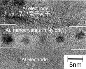
![[ABSTRACT]](logo312.gif) Very thin Nylon 11 films (≤20 nm in thickness) containing Au nanoparticles were prepared, and current–voltage (I–V) characteristics in the vertical direction of the films were studied. The plan and cross-sectional transmission electron microscopic images revealed that Au particles are spontaneously aligned in the middle of the upper and lower electrodes and Nylon 11 tunneling barriers are naturally formed between Au nanoparticles and electrodes. Clear Coulomb staircases were observed in the I–V characteristics. Very thin Nylon 11 films (≤20 nm in thickness) containing Au nanoparticles were prepared, and current–voltage (I–V) characteristics in the vertical direction of the films were studied. The plan and cross-sectional transmission electron microscopic images revealed that Au particles are spontaneously aligned in the middle of the upper and lower electrodes and Nylon 11 tunneling barriers are naturally formed between Au nanoparticles and electrodes. Clear Coulomb staircases were observed in the I–V characteristics. |
|
 |
28. Yoku Inoue, Atsushi Tanaka, Minoru Fujii, Shinji Hayashi and Keiichi Yamamoto,
"Single-electron
Tunneling Through Si Nanocrystals Dispersed in Phosphosilicate Glass Thin Films,”
Journal of Applied Physics, Vol. 86, No. 6, pp.3199-3203, September (1999) |
| Electrical transport properties of extremely thin phosphosilicate glass
(PSG) films containing Si nanocrystals (nc-Si) a few nanometers in diameter
were studied. Samples were prepared by cosputtering Si and PSG targets,
and post annealing. Periodic Coulomb staircases were clearly observed in
the dc current–voltage (I–V) characteristics along the vertical direction
of films. Although the step structure was broadened with increasing the
temperature, it remained up to 200 K. The I–V curve could be well fitted
by Monte Carlo simulation with a simple double-barrier structure model.
Advantages of using PSG instead of SiO2 as surrounding matrices of nc-Si
to observe single-electron tunneling effects are discussed. |
|
|
25. Yoku Inoue, Makoto Inata, Minoru Fujii, Shinji Hayashi and Keiichi
Yamamoto,
"Single Electron Tunneling in Thin Metal Granular Films,”
Thin Solid Films, Vol. 349, No. 1-2, pp.289-292, July (1999).
|
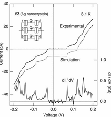
| Electrical transport properties of extremely thin metal (Ag and Au) granular
films fabricated by a cosputtering method were studied. High-resolution
transmission electron microscopic observations revealed that Ag (Au) nanocrystals
several nanometers in diameter were dispersed in thin films. In spite of
the large size (100×100 μm2) of the devices prepared, the Coulomb blockade
and the Coulomb staircase were observed on current–voltage (I–V) characteristics
at relatively high temperature (100 K). Although the samples were prepared
under the same conditions, the I–V curves varied from sample to sample.
The observed I–V curves were well fitted by Monte Carlo simulation assuming
that the samples consist of a few serial and parallel connections of nanocrystals.
The present results suggest that the macroscopic conduction of thin granular
films is dominated by only a few special conduction paths. |
|
| |
|
|
|